
User Manual


DS899F1 6
CS4234
1. PIN DESCRIPTIONS
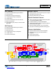
Figure 1. CS4234 Pinout
Pin Name Pin # Pin Description
SDA 1
Serial Control Data (Input/Output) - Bidirectional data I/O for the I²C
TM
control port.
SDINx 2,3 Serial Data Input (Input) - Input channels serial audio and low latency data.
FS/LRCK 4
Frame Synchronization Clock/Left/Right Clock (Input/Output) - Determines which channel or
frame is currently active on the serial audio data line.
MCLK 5 Master Clock (Input) -Clock source for the internal logic, processing, and modulators.
SCLK 6 Serial Clock (Input/Output) -Serial Clock for the serial data port.
SDOUT1 7
Serial Data Output 1 (Output) - ADC data output into a multi-slot TDM stream or AIN1 and AIN2
ADC data output in Left Justified and I²S modes.
VL 8 Interface Power (Input) - Positive power for the digital interface level shifters.
GND 9,21
Ground (Input) - Ground reference for the I/O and digital, analog sections.
VDREG 10 Digital Power (Output) - Internally generated positive power supply for digital section.
AINx+
11,13,15,
17
Positive Analog Input (Input) - Positive input signals to the internal analog to digital converters.
The full scale analog input level is specified in the Analog Input Characteristics table.
AINx-
12,14,16,
18
Negative Analog Input (Input) - Negative input signals to the internal analog to digital converters.
The full scale analog input level is specified in the Analog Input Characteristics table.
FILT+ 19 Positive Voltage Reference (Output) - Positive reference voltage for the internal ADCs.
VA 20 Analog Power (Input) - Positive power for the analog sections.
VQ 22 Quiescent Voltage (Output) - Filter connection for internal quiescent voltage.
VREF 23 Analog Power Reference (Input) - Return pin for the VBIAS cap.
AD0
AD2/SDOUT2
AOUT5+
VA
AIN3+
AIN4-
AIN3-
AIN2+
AIN2-
AIN1-
AIN1+
FILT+
SDA
MCLK
SDOUT1
VL
GND
SDIN1
SDIN2
12
11
13
14
15
16
17
18
19
20
29
30
28
27
26
25
24
23
22
21
39
40
38
37
36
35
34
33
32
31
2
1
3
4
5
6
7
8
9
10
AOUT1+
SCLK
VDREG
AOUT2+
AOUT2-
AOUT3+
AOUT3-
AOUT4-
AOUT4+
VBIAS
VREF
VQ
GND
AOUT5-
AOUT1-
SCL
FS/LRCK
AD1
INT
RST
AIN4+
Top-Down
(Though Package)
View