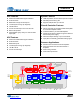
CS4234 4 In/5 Out CODEC with Programmable Class H Controller DAC Features System Features Advanced multibit Delta–Sigma modulator TDM, left justified, and I2S serial inputs and outputs 24-bit resolution Nondelayed low-latency path Differential or single-ended outputs Supports sample rates up to 96 kHz -109 dB dynamic range (A-weighted) Class H Controller Features -90 dB THD+N Can be used with any integrated Class AB amplifier IC or discrete amplifier solution.
CS4234 General Description The CS4234 is a highly versatile CODEC that combines 4 channels of high performance analog to digital conversion, 4 channels of high performance digital to analog conversion for audio, and 1 channel of digital to analog conversion to provide a nondelayed audio reference signal to an external Class H tracking power supply.
CS4234 TABLE OF CONTENTS 1. PIN DESCRIPTIONS ............................................................................................................................ 6 1.1 I/O Pin Characteristics ..................................................................................................................... 7 2. TYPICAL CONNECTION DIAGRAM ................................................................................................... 8 3. CHARACTERISTICS AND SPECIFICATIONS ......................
CS4234 6.25 Interrupt Notification 2 (Address 22h) (Read Only) ...................................................................... 69 7. ADC FILTER PLOTS ............................................................................................................................ 70 8. DAC FILTER PLOTS ............................................................................................................................ 71 9. PACKAGE DIMENSIONS .........................................................
CS4234 Figure 41. SSM DAC Passband Ripple .................................................................................................... 71 Figure 42. DSM DAC Stopband Rejection ................................................................................................ 72 Figure 43. DSM DAC Transition Band ...................................................................................................... 72 Figure 44. DSM DAC Transition Band (Detail) ...........................................
CS4234 SCL AD0 AD1 AD2/SDOUT2 INT RST AOUT5+ AOUT5- AOUT1+ AOUT1- 40 39 38 37 36 35 34 33 32 31 1. PIN DESCRIPTIONS SDA 1 30 AOUT2+ SDIN1 2 29 AOUT2- SDIN2 3 28 AOUT3+ FS/LRCK 4 27 AOUT3- MCLK 5 26 AOUT4+ SCLK 6 25 AOUT4- SDOUT1 7 24 VBIAS Top-Down (Though Package) View 18 19 20 AIN1- FILT+ VA 16 AIN2- 17 15 AIN2+ AIN1+ 14 GND AIN3- 21 13 10 AIN3+ VQ VDREG 12 VREF 22 AIN4- 23 9 11 8 AIN4+ VL GND Figure 1.
CS4234 Pin Name Pin # VBIAS 24 Pin Description Positive Voltage Reference (Output) - Positive reference voltage for the internal DACs. AOUTx- 25,27,29, Negative Analog Output (Output) - Negative output signals from the internal digital to analog con31, 33 verters. The full scale analog output level is specified in the Analog Output Characteristics table. AOUTx+ 26,28,30, Positive Analog Output (Output) - Positive output signals from the internal digital to analog con32, 34 verters.
0.1 uF 5.0 VD C 0 .1u F 1 0u F S CL K S DO UT1 6 7 10 9 V DR EG GN D RT 13 C S4234 12 M C LK 5 11 FS/ LR C K 4 VL S DI N2 3 8 S DI N1 40 SCL AIN 4+ 2 39 AD 0 AIN 4- S DA 37 38 AD 1 AIN 3+ 1 32 33 34 35 36 INT AD 2 Pull Up or Down B as ed upon Desired A ddress .
CS4234 3. CHARACTERISTICS AND SPECIFICATIONS RECOMMENDED OPERATING CONDITIONS GND = 0 V; all voltages with respect to ground. (Note 3) Parameters Symbol Min Typ Max Units Analog Core VA 3.135 4.75 3.3 5 3.465 5.25 V V Level Translator VL 1.71 - 5.25 V Ambient Operating Temperature - Power Applied TA -40 - +105 C Junction Temperature TJ -40 - +150 C DC Power Supply Temperature Notes: 3. Device functional operation is guaranteed within these limits.
CS4234 DC ELECTRICAL CHARACTERISTICS GND = 0 V; all voltages with respect to ground. Parameters Min Typ Max Units - 2.5 0.5 - V - VA 23 - 1 V k A - 0.5•VA 77 - 0 V k A VDREG (Note 7) Nominal Voltage Output Impedance FILT+ Nominal Voltage Output Impedance DC Current Source/Sink VQ Nominal Voltage Output Impedance DC Current Source/Sink Notes: 7. No external loads should be connected to the VDREG pin.
CS4234 TYPICAL CURRENT CONSUMPTION This table represents the power consumption for individual circuit blocks within the CS4234. CS4234 is configured as shown in Figure 2 on page 8. VA_SEL = 0 for VA = 3.3 VDC, 1 for VA = 5.0 VDC; FS = 100 kHz; MCLK = 25.6 MHz; DAC load is 3 k; All input signals are zero (digital zero for SDINx inputs and AC coupled to ground for AINx inputs) .
CS4234 ANALOG INPUT CHARACTERISTICS Test Conditions (unless otherwise specified): Device configured as shown in Figure 2 on page 8. Input sine wave: 1 kHz; VA_SEL = 0 for VA = 3.3 VDC, 1 for VA = 5.0 VDC.; TA = -40 to +105 C; Measurement Bandwidth is 20 Hz to 20 kHz unless otherwise specified; Sample Rate = 48 kHz; all Power Down ADCx bits = 0. VA, VREF = 3.3 V Parameter Min VA, VREF = 5.
CS4234 634 470 pF VA 4.7 uF - 90.9 CS4234 AINx + 100 k Analog Signal + 100 k 100 k + 2700 pF 100 k 100 k + Analog Signal 100 k 4.7 uF CS4234 AINx 90.9 - VA 470 pF 634 Figure 3. Test Circuit for ADC Performance Testing +Vcc +Vcc Operational Amplifier Power DAC DUT PWR + OUT GND GND -Vcc Analog Out - + - + OUT Analog Generator Digital Out - + Analyzer Test Equipment Figure 4.
CS4234 ADC DIGITAL FILTER CHARACTERISTICS Test Conditions (unless otherwise specified): Device configured as shown in Section 2. on page 8. Input sine wave: 1 kHz; VA_SEL = 0 for VA = 3.3 VDC, 1 for VA = 5.0 VDC.; TA = -40 to +105 C; Measurement Bandwidth is 20 Hz to 20 kHz unless otherwise specified. See filter plots in Section 7. on page 70. Parameter (Note 15) Passband (Frequency Response) to -0.1 dB corner Passband Ripple Min Typ Max Unit 0 - 0.4535 Fs -0.09 - 0.17 dB Stopband 0.
CS4234 ANALOG OUTPUT CHARACTERISTICS Test Conditions (unless otherwise specified): Device configured as shown in Section 2. on page 8. VA_SEL = 0 for VA = 3.3 VDC, 1 for VA = 5.0 VDC.; TA = -40 to +105 C; Full-scale 1 kHz input sine wave; Sample Rate = 48 kHz; Measurement Bandwidth is 20 Hz to 20 kHz; Specifications apply to all channels unless otherwise indicated; all Power Down DACx bits = 0. See (Note 19). VA, VREF= 3.3 V (Differential/Single-ended) Parameter VA, VREF= 5.
CS4234 COMBINED DAC INTERPOLATION AND ON-CHIP ANALOG FILTER RESPONSE Test Conditions (unless otherwise specified): VA_SEL = 0 for VA = 3.3 VDC, 1 for VA = 5.0 VDC. The filter characteristics have been normalized to the sample rate (FS) and can be referenced to the desired sample rate by multiplying the given characteristic by FS. See filter plots in Section 8. on page 71.
CS4234 DIGITAL I/O CHARACTERISTICS Parameters High-Level Input Voltage (all input pins except RST) (% of VL) (VL = 1.8 V) High-Level Input Voltage (all input pins except RST) (% of VL) (VL = 2.5 V, 3.3 V, or 5 V) Low-Level Input Voltage (all input pins except RST) (% of VL) High-Level Input Voltage (RST pin) Low-Level Input Voltage (RST pin) Symbol Min Typ Max Units VIH 75% - - V VIH 70% - - V VIL - - 30% V VIH 1.2 - - V VIL - - 0.
CS4234 SWITCHING CHARACTERISTICS - SERIAL AUDIO INTERFACE VA_SEL = 0 for VA = 3.3 VDC, 1 for VA = 5.0 VDC. Parameters RST pin Low Pulse Width (Note 26) MCLK Frequency MCLK Duty Cycle SCLK Duty Cycle Input Sample Rate (FS/LRCK pin) (Note 27) Single-Speed Mode Double-Speed Mode SCLK Falling Edge to SDOUTx Valid (VL = 1.8 V) SCLK Falling Edge to SDOUTx Valid (VL = 2.5 V) SCLK Falling Edge to SDOUTx Valid (VL = 3.
CS4234 ~ ~ ~ tLPW FS/LRCK (input) tlcks SCLK (input) tds tdh1 SDINx MSB (input) tdh2 MSB-1 tdh2 SDOUT1 MSB (output) MSB-1 Figure 6. TDM Serial Audio Interface Timing FS/LRCK (input/output) tlcks SCLK (input/output) tds SDINx (input) tdh1 MSB MSB-1 MSB MSB-1 tdh2 SDOUTx (output) Figure 7.
CS4234 SWITCHING SPECIFICATIONS - CONTROL PORT Test conditions (unless otherwise specified): Inputs: Logic 0 = GND = 0 V, Logic 1 = VL; SDA load capacitance equal to maximum value of Cb specified below (Note 31). Parameters Symbol Min Max Unit SCL Clock Frequency fscl - 550 kHz RESET Rising Edge to Start tirs (Note 32) - ns Bus Free Time Between Transmissions tbuf 1.3 - µs Start Condition Hold Time (prior to first clock pulse) thdst 0.6 - µs Clock Low time tlow 1.
CS4234 4. APPLICATIONS 4.1 Power Supply Decoupling, Grounding, and PCB Layout As with any high-resolution converter, the CS4234 requires careful attention to power supply and grounding arrangements if its potential performance is to be realized. Figure 2 shows the recommended power arrangements, with VA connected to clean supplies. VDREG, which powers the digital circuitry, is generated internally from an on-chip regulator from the VA supply.
CS4234 4.2.2 Power-down To prevent audio transients at power-down, the DC-blocking capacitors must fully discharge before turning off the power. In order to do this in a controlled manner, it is recommended that all the converters be muted to start the sequence. Next, set PDNx for all converters to 1 to power them down internally. Then, FS/LRCK and SCLK can be removed if desired.
CS4234 System Unpowered Apply VL, VA, and MCLK Remove VL, VA, and MCLK 250 ms VQ Ready (> 90% of Typical) Set RST 2 2 ms + (3000/MCLK) Write all required configuration settings to Control Port 2 ms + (3000 /MCLK) I C Address Captured & Control Port Ready Clear RST 50 ms Set VQ_RAMP bit Write VA_SEL bit (in 0Fh) appropriately for VA 250ms Start SCLK, FS/LRCK, SDINx Stop SCLK, FS/LRCK, SDINx Clear PDN DACx & ADCx bits Set all PDN DAC & ADC bits Clear reset to SMPS controller Set PDN_CHx bits R
CS4234 4.2.3 DAC DC Loading Figure 10 shows the analog output configuration during power-up, with the AOUTx± pins clamped to VQ to prevent pops and clicks. Thus any DC loads (RLx) on the output pins will be in parallel when the switches are closed. These DC loads will pull the VQ voltage down towards ground. If the parallel combination of all DC loads exceeds the specification shown in the Analog Output Characteristics table, the VQ voltage will never rise to its minimum operating voltage.
CS4234 4.3 I²C Control Port All device configuration is achieved via the I²C control port registers as described in the Switching Specifications - Control Port table. The operation via the control port may be completely asynchronous with respect to the audio sample rates. However, to avoid potential interference problems, the I²C pins should remain static if no operation is required. The CS4234 acts as an I²C slave device. SDA is a bidirectional data line.
CS4234 Receive acknowledge bit. Send stop condition, aborting write. Send start condition. Send 0010xxx1 (chip address and read operation). Receive acknowledge bit. Receive byte, contents of selected register. Send acknowledge bit. Send stop condition. Setting the auto increment bit in the MAP allows successive reads or writes of consecutive registers. Each byte is separated by an acknowledge bit. 4.3.
CS4234 FS/LRCK (kHz) MCLK (MHz) 128x (Note 34) 192x (Note 34) 256x 384x 512x 32 - - 8.1920 12.2880 16.3840 44.1 - - 11.2896 16.9344 22.5792 48 - - 12.2880 18.4320 24.5760 64 8.1920 12.2880 16.3840 - - 88.2 11.2896 16.9344 22.5792 - - 96 12.2880 18.4320 24.5760 - - DSM Mode SSM Table 2. Common Clock Frequencies Note: 34. 128x and 192x ratios valid only in Left Justified or I²S formats. 4.4.
CS4234 The serial bit clock, SCLK, must be synchronously derived from the master clock, MCLK, and be equal to 512x, 256x, 128x, 64x, 48x or 32x FS, depending on the desired format and speed mode. Refer to Table 4 and Table 5 for required clock ratios. SSM DSM MCLK/FS 256x, 384x, 512x 128x, 192x, 256x SCLK/FS 32x, 48x, 64x, 128x 32x, 48x, 64x Table 4. Slave Mode Left Justified and I²S Clock Ratios (Note 35) SSM DSM MCLK/FS 256x, 384x, 512x 512x 256x SCLK/FS 256x 512x 256x Table 5.
CS4234 32-Bit Channel Block MSB -1 -2 -3 -4 -5 -6 -7 +3 +2 +1 LSB 24-Bit Audio Word 8-Bit Zero Pad (Or DAC5 Data) Figure 15. 32-bit Receiver Channel Block The structure in which the serial data is coded into the TDM slots is shown in Figure 16. When using a 48 kHz sample rate with a 24.576 MHz MCLK and SCLK, a 16 slot TDM structure can be realized. When using a 48 kHz sample rate with 12.288 MHz SCLK and 24.576 MHz MCLK, or a 96 kHz sample rate with a 24.
DS899F1 SDOUT with ADC1 Sidechain Data[31:8] Input Data 1.1.B [7:0] x [7:0] 0's [7:0] 0's [7:0] Input Data 1.1.A [31:8] Input Data 2.1 [31:8] ADC1 Data [31:8] SDIN1 SDIN2 SDOUT SDOUT with ADC1 Data [31:8] Sidechain …→… 0's [7:0] SDOUT Slot 1 [31:0] ADC2 Data [31:8] 0's [7:0] ADC1 Data[31:8] SDIN2 0's [7:0] 0's [7:0] x [7:0] 0's [7:0] FS = 48kHz x [7:0] Output Data (SDIN2 Slot 4) Input Data 2.8 [31:8] x [7:0] Slot 8 [31:0] Input Data 1.8.
CS4234 4.5.2 Left Justified and I²S Modes The serial port of the CS4234 supports the Left Justified and I²S interface formats with valid bit depths of 16, 18, 20, or 24 bits for the SDOUTx pins and 24 bits for the SDINx pins. All data is valid on the rising edge of SCLK. Data is clocked out of the ADC on the falling edge of SCLK and clocked into the DAC on the rising edge. In Master Mode each slot is 32 bits wide.
CS4234 4.6 Internal Signal Path VA 5.0 VDC VD 2. 5 VDC -1 -2 2.5 V Gain / Volume Tracking SMPS Enable Max Detect Envelope Tracking Mute, Invert , Noise Gate TPS GAIN X DAC Volume X Master Vol .
CS4234 DSP DSP Device D x Device D SDOUT1 x SDIN2 x SDIN1 x Each of the device’s ADC data is reflected in the TDM stream on SDOUT1 and then routed to the system controller.
DS899F1 Slots 13-16 of SDIN2 111 Slot 1 [31: 0] Slot 1 [31: 0] SDIN1 SDIN2 …→… Slots 9-12 of SDIN2 110 Slot 5 [31:0] Slot 5 [31:0] Slot 3 [31:0] Slot 3 [31:0] …→… Slot 8 [31:0] Slot 8 [31:0] SCLK = 24 .576 MHz FS/LRCK = 48 kHz MCLK = 24.576MHz Slot 4 [31:0] Slot 9 [31:0] Slot 9 [31:0] Slot 5 [31:0] SCLK = 12.288/24.576MHz Slot 4 [31:0] Slot 5 [31:0] MCLK = 12.288/24.
DS899F1 Slots 5-8 of SDIN1 Slots 9-12 of SDIN1 Slots 13-16 of SDIN1 Slots 1-4 of SDIN2 Slots 5-8 of SDIN2 Slots 9-12 of SDIN2 Slots 13-16 of SDIN2 001 010 011 100 101 110 111 SDIN2 Slots 5-8 of SDIN1 Slots 9-12 of SDIN1 Slots 13-16 of SDIN1 Slots 1-4 of SDIN2 Slots 5-8 of SDIN2 Slots 9-12 of SDIN2 Slots 13-16 of SDIN2 001 010 011 100 101 110 111 DAC5 [23:0] x SDIN1 SDIN2 x x x Slot 2 [31:0] Slots 1-4 of SDIN1 000 Slot 1 [31:0] DAC1-4 Data is in: DAC1-4 Source [2:0] LL4 [23 :0] x
CS4234 As can be seen from Figure 22, setting ‘100’ of the DAC5 Source[2:0] bits configures the DAC5 path to use the mask bits to determine which signals are routed into the DAC5 path. The CS4234 is designed to make any one of the slots of both the SDINx pins available to the 5th DAC Input Advisory block, where the mask bits for the DAC5 path are located. The configuration of the mask bits is shown in Table 6 and Table 7.
CS4234 SDIN2 Mask 1[7:0] Setting Data to be Unmasked from DAC5 Path x x x SDIN2 Mask 2[7:0] Setting SDIN2 Slot 1 0 x x x x x x x x x x x x SDIN2 Slot 2 x 0 x x x x x x x x x x x x x x SDIN2 Slot 3 x x 0 x x x x x x x x x x x x x SDIN2 Slot 4 x x x 0 x x x x x x x x x x x x SDIN2 Slot 5 x x x x 0 x x x x x x x x x x x SDIN2 Slot 6 x x x x x 0 x x x x x x x x x x SDIN2 Slot 7 x x x x x x 0 x x x
CS4234 4.6.2 ADC Path VD 2.5 VDC VA 5. 0 VDC -1 -2 2.5 V DC Offset Gain / Volume Tracking SMPS Enable Max Detect Envelope Tracking Mute, Invert , Noise Gate TPS GAIN X DAC Volume X Master Vol .
CS4234 4.6.3 DAC1-4 Path VA 5.0 VDC VD 2.5 VDC -1 -2 2.5 V Tracking SMPS Enable Max Detect Envelope Tracking Mute, Invert, Noise Gate TPS GAIN X DAC Volume X Master Vol .
CS4234 The de-emphasis feature is included to accommodate audio recordings that utilize 50/15 s preemphasis equalization as a means of noise reduction. De-emphasis is only available in Single-speed Mode. Gain dB T1=50 µs 0dB T2 = 15 µs -10dB F1 3.183 kHz F2 Frequency 10.61 kHz Figure 25. De-emphasis Curve 4.6.4 Low-Latency Path VD 2.5 VDC VA 5.0 VDC -1 -2 2.
CS4234 4.6.5 DAC5 Path VD 2.5 VDC VA 5.0 VDC -1 -2 2.5 V Gain / Volume Tracking SMPS Enable Max Detect Envelope Tracking Mute, Invert, Noise Gate TPS GAIN X DAC Volume X Master Vol .
CS4234 4.6.5.2 Generating the Tracking Signal Inside an External DSP If the tracking signal is to be generated within an external DSP, the tracking signal generation blocks mentioned above can be bypassed by setting the “DAC5 CFG & FLTR[1:0]” bits in the "DAC Control 1" register to either the interpolation filter option (‘00’) or the sample and hold filter (’01’).
CS4234 control and other associated peripheries for DAC1-4 is shown in Figure 28 below. The implementation details for the volume control and other associated peripheries for the DAC5 path is shown in Figure 29. INV.
CS4234 4.6.6.2 Soft Ramp The CS4234 soft ramp feature (enabled using the DAC1-4 ATT. and DAC5 ATT. bits) is activated on mute and unmute transitions as well as any normal volume register changes. To avoid any potential audible artifacts due to the soft ramping, the volume control algorithm implements the ramping function differently based upon how the user attempts to control the volume.
CS4234 Wait State Envelope Counter Running USER: Change Volume or Mute Register Envelope Counter Timed Out? Yes Reset Envelope Counter No Reset Envelope Counter Ramp Rate Ramp Rate = MUTE_DELAY New Volume Setting - Current Volume Setting Time Between Volume Changes MIN_DELAY Limit Ramp Rate MAX_DELAY Figure 30. Soft Ramp Behavior Two control parameters allow the user to limit the ramp-rate range to achieve optimum effect.
CS4234 Fs = 48 kHz or 96 kHz (Base = 48 kHz) Ramp Rate Time to Ramp Time to Ramp to Full Scale 6 dB (ms) (ms) ms/dB 1 x Base 21.33 1.33 0.22 2 x Base 42.67 2.67 4 x Base 85.33 5.33 8 x Base 170.67 16 x Base 341.33 Fs = 32 kHz or 64 kHz (Base = 32 kHz) Time to Ramp Time to Ramp to Full Scale 6 dB (ms) (ms) ms/dB 32 2 0.33 0.44 64 4 0.66 0.89 128 8 1.33 10.67 1.77 256 16 2.66 21.33 3.54 512 32 5.32 32 x Base 682.67 42.67 7.09 1024 64 10.63 64 x Base 1365.33 85.
CS4234 4.7 Reset Line The reset line of the CS4234 is used to place the device into a reset condition. In this condition, all of the values of the CS4234 control port are set to their default values. This mode of operation is the lowest power mode of operation for the CS4234 and should be used whenever the device is not operating in order to save power.
CS4234 gardless of the setting of the mask bit. Setting the mask bit only prevents the interrupt pin from being flagged upon the occurrence. 4.8.2 Interrupt Line Operation As mentioned previously, the interrupt line of the CS4234 will be pulled low or high (depending on the settings of the “INT PIN[1:0]” bits in the "Interrupt Control" register) after an interrupt condition occurs, provided that the event is not masked in the mask register.
CS4234 USER: Mask bit(s) set to 0 New Unmasked Error New Unmasked Error New Unmasked Error New Unmasked Error New Unmasked Error New Unmasked Error Unmasked error occurs Status Register bit changes to ‘1’ and INT pin set to active level USER: Read Status Registers (see status bit(s) = ‘1’) Mask bit(s) of corresponding status bit(s) set to ‘1’ INT pin set to inactive level Status Register bit(s) set to ‘1’ USER: Takes Corrective Action All Status Register bits cleared Are any errors still occ
CS4234 5. REGISTER QUICK REFERENCE Default values are shown below the bit names. AD Function 7 6 5 4 3 2 1 0 1 0 0 0 0 0 0 0 (Read Only Bits are shown in Italics) 01h p 52 02h p 52 03h p 52 04h 05h p 52 06h p 53 07h p 54 08h Device ID A and B Device ID C and D Device ID E and F Variant ID Revision ID Clock and SP Sel. Sample Width Sel. SP Control p 55 09h p 56 0Ah p 57 0Bh p 57 0Ch p 58 0Dh p 58 0Eh p 59 0Fh p 60 10h p 61 11h p 61 12h p 62 13h p 63 14h p 63 15h p 64 SP Data Sel.
CS4234 AD Function 7 6 5 4 3 2 1 0 (Read Only Bits are shown in Italics) 16h p 65 17h p 66 18h p 66 19h p 66 1Ah p 66 1Bh p 66 1Ch p 66 1Dh Volume Mode Master Volume DAC1 Volume DAC2 Volume DAC3 Volume DAC4 Volume DAC5 Volume MUTE DELAY[1:0] 1 p 66 1Fh Interrupt Control Interrupt Mask 1 p 68 21h p 68 22h p 69 Interrupt Mask 2 0 0 0 0 0 0 0 0 0 1 1 1 1 0 0 0 0 0 0 0 0 0 0 0 0 0 0 0 0 0 0 DAC1 VOLUME[7:0] 1 0 DAC2 VOLUME[7:0] 0 0 0 1 0 DAC3 VOLUME[7:0] 0
CS4234 6. REGISTER DESCRIPTIONS All registers are read/write unless otherwise stated. All “Reserved” bits must maintain their default state. Default values are shaded. 6.1 Device I.D. A and B (Address 01h) (Read Only) Device I.D. C and D (Address 02h) (Read Only) Device I.D. E and F (Address 03h) (Read Only) 7 6 5 4 3 2 DEV. ID A[3:0] 7 6 5 4 3 2 DEV. ID C[3:0] 7 6 0 1 0 1 0 DEV. ID D[3:0] 5 4 3 2 DEV. ID E[3:0] 6.1.1 1 DEV. ID B[3:0] DEV. ID F[3:0] Device I.D.
CS4234 6.3 Clock and SP Select (Address 06h) 7 6 BASE RATE[1:0] 6.3.1 5 4 SPEED MODE[1:0] 3 2 MCLK RATE[2:0] 1 0 Reserved Base Rate Advisory Advises the CS4234 of the base rate of the incoming base rate. This allows for the de-emphasis filters to be adjusted appropriately and the group delay block for the DAC1-4 path to be calculated correctly. The CS4234 includes on-chip digital de-emphasis for 32, 44.1, and 48 kHz base rates. It is not supported for 96 kHz or for any settings in Double Speed Mode.
CS4234 6.4 Sample Width Select (Address 07h) 7 6 SDOUTx SW[1:0] 6.4.1 5 4 INPUT SW[1:0] 3 2 LOW LAT. SW[1:0] 1 0 DAC5 SW[1:0] Output Sample Width These bits set the width of the samples placed into the outgoing SDOUTx streams. OUTPUT SW Sample Width is: 00 16 bits 01 18 bits 10 20 bits 11 24 bits Note: Bits which are wider than the Output Sample Width setting above will be set to zero within the SDOUTx data stream. 6.4.
CS4234 6.5 Serial Port Control (Address 08h) 7 INV SCLK 6.5.1 6 5 DAC5 SOURCE[2:0] 4 3 2 SP FORMAT[1:0] 1 0 SDO CHAIN MASTER/SLAVE Invert SCLK When set, this bit inverts the polarity of the SCLK signal. 6.5.2 INV SCLK SCLK is: 0 Not Inverted 1 Inverted DAC5 Input Source Sets which portion of data is to be routed to the DAC5 data path. 6.5.
CS4234 6.6 Serial Port Data Select (Address 09h) 7 Reserved 6.6.1 6 Reserved 5 4 DAC1-4 SOURCE[2:0] 3 2 1 LL SOURCE[2:0] 0 DAC1-4 Data Source Sets which portion of data is to be routed to the DAC1-4 data paths. DAC1-4 SOURCE Data is routed into the DAC1-4 path from: 6.6.
CS4234 6.7 Serial Data Input 1 Mask 1 (Address 0Ah) 7 6 6.7.1 5 4 3 SDIN1 MASK 1[7:0] 2 1 0 SDIN1 Mask 1 This field determines what data is masked from the max detect and envelope tracking blocks in the DAC5 data path. 6.8 SDIN1 MASK 1 Unmasked Data (in addition to any other data that is unmasked by its respective mask bits): 11111111 All Data is Masked. 0xxxxxxx Slot 1 of SDIN1. x0xxxxxx Slot 2 of SDIN1. xx0xxxxx Slot 3 of SDIN1. xxx0xxxx Slot 4 of SDIN1. xxxx0xxx Slot 5 of SDIN1.
CS4234 6.9 Serial Data Input 2 Mask 1 (Address 0Ch) 7 6 6.9.1 5 4 3 SDIN2 MASK 1[7:0] 2 1 0 SDIN2 Mask 1 This field determines what data is masked from the max detect and envelope tracking blocks in the DAC5 data path. 6.10 SDIN2 MASK 1 Unmasked Data (in addition to any other data that is unmasked by its respective mask bits): 11111111 All Data is Masked. 0xxxxxxx Slot 1 of SDIN2. x0xxxxxx Slot 2 of SDIN2. xx0xxxxx Slot 3 of SDIN2. xxx0xxxx Slot 4 of SDIN2. xxxx0xxx Slot 5 of SDIN2.
CS4234 6.11 Tracking Power Supply Control (Address 0Eh) 7 TPS MODE 6.11.1 6 5 TPS OFFSET[2:0] 4 3 2 1 GROUP DELAY[3:0] 0 Tracking Power Supply Mode If DAC5 FLTR (Section 6.15.5) is set to Tracking Power Supply Mode, setting this bit changes the reference of the DAC5 output from 0 V to full-scale output voltage.
CS4234 6.11.3 Group Delay Sets the group delay added to the DAC1-4 path. This delay is in addition to any inherent delay in the DAC. Modify these bits only while all of the ADCs and DACs are powered down and the DACs are in mute state. GROUP DELAY [3:0] Nominal Group Delay [s] Sample Rate Sample Rate Sample Rate Sample Rate Sample Rate Sample Rate 32 kHz 44.1 kHz 48 kHz 64 kHz 88.
CS4234 6.13 ADC Control 2 (Address 10h) 7 MUTE ADC4 6 MUTE ADC3 5 MUTE_ADC2 4 MUTE ADC1 3 PDN ADC4 2 PDN ADC3 1 PDN ADC2 0 PDN ADC1 2 INV. LL3 1 INV. LL2 0 INV. LL1 6.13.1 Mute ADCx Mutes the ADCx signal MUTE ADCx ADC is: 0 Not Muted 1 Muted 6.13.2 Power Down ADCx Powers down the ADCx path. 6.14 PDN ADCx ADC is: 0 Powered Up 1 Powered Down Low Latency Path Control (Address 11h) 7 6 LL NG[2:0] 5 4 Reserved 3 INV. LL4 6.14.
CS4234 6.15 DAC Control 1 (Address 12h) 7 6 DAC1-4 NG 5 4 DAC1-4 DE 3 DAC5 DE 2 DAC5 MVC 1 0 DAC5 CFG & FLTR[1:0] 6.15.1 DAC1-4 Noise Gate This sets the bit depth at which the Noise Gate feature should engage for the DAC1-4 path. DAC1-4 NG[2:0] Noise Gate is set at: [b] 000 Upper 13 Bits (72 dB) 001 Upper 14 Bits (78 dB) 010 Upper 15 Bits (84 dB) 011 Upper 16 Bits (90 dB) 100 Upper 17 Bits (96 dB) 101 Upper 18 Bits (102 dB) 110 Upper 24 Bits (138 dB) 111 Noise Gate Disabled 6.15.
CS4234 6.15.5 DAC5 Configuration and Filter Selection Selects the filtering applied to the DAC5 data or configures the DAC5 Path used to generate a tracking power supply reference. If placed into Tracking Power Supply mode, an interpolation filter is applied to the outgoing data; otherwise, either an interpolation or a sample-and-hold filter can be applied to the path. 6.16 DAC5 FLTR Filter Selected is: 00 Interpolation Filter 01 Sample and Hold 10 Tracking Power Supply Mode (See Section 4.6.5.
CS4234 6.17.2 DAC1-4 Attenuation Sets the mode of attenuation used for the DAC1-4 path. DAC1-4 ATT Attenuation events happen: 0 On a soft ramp 1 Immediately Note: See Section 4.6.6 Volume Control for details regarding the attenuation modes. 6.17.3 Mute Low-latency Path Mutes the low-latency path. MUTE LL Low latency path is: 0 Not Muted 1 Muted 6.17.4 Mute DACx Mutes the DACx signal. 6.
CS4234 6.19 Volume Mode (Address 16h) 7 6 MUTE DELAY[1:0] 5 4 MIN DELAY[2:0] 3 2 1 MAX DELAY[2:0] 0 6.19.1 Mute Delay Sets the delay between the volume steps during the muting and unmuting of a signal when the attenuation mode is set to soft ramp. Each step of the ramp is equal to 6.02/64 dB ~= 0.094 dB. Settings are given as “x” times the base period. MUTE DELAY Delay is: 00 1x 01 4x 10 16x 11 64x 6.19.2 Minimum Delay Sets the minimum delay before each volume transition.
CS4234 6.20 Master and DAC1-5 Volume Control (Address 17h, 18h, 19h, 1Ah, 1Bh, and 1Ch) 7 6 5 4 3 x VOLUME[7:0] 2 1 0 6.20.1 x Volume Control Sets the level of the x Volume Control. Each volume step equals 6.02/16 dB ~= 0.38 dB. See Section 4.6.6.1 on page 43 for the muting behavior of these volume registers. 6.21 x VOLUME x Volume is: [dB] 00000000 +6.02 00001111 +0.38 00010000 0 00010001 -0.38 00011000 -3.01 ... ... 11101100 -82.
CS4234 6.22 Interrupt Mask 1 (Address 1Fh) 7 MASK TST MODE ERR 6 MASK SP ERR 5 MASK CLK ERR 4 Reserved 3 MASK ADC4 OVFL 2 MASK ADC3 OVFL 1 MASK ADC2 OVFL 0 MASK ADC1 OVFL 6.22.1 Test Mode Error Interrupt Mask Allows or prevents a Test Mode Error event from flagging the interrupt pin. A test mode error occurs when an inadvertent I²C write places the device in test mode. MASK TST MODE ERR In the event of a Test Mode Error event, Interrupt Pin will: 0 Be Flagged 1 Not be flagged 6.22.
CS4234 6.23 Interrupt Mask 2 (Address 20h) 7 6 Reserved Reserved 5 4 3 2 1 0 Reserved MASK DAC5 CLIP MASK DAC4 CLIP MASK DAC3 CLIP MASK DAC2 CLIP MASK DAC1 CLIP 6.23.1 DACx Clip Interrupt Mask Allows or prevents a DACx Clip event from flagging the interrupt pin. MASK DACx CLIP 6.
CS4234 6.25 Interrupt Notification 2 (Address 22h) (Read Only) 7 6 5 4 3 2 1 0 Reserved Reserved Reserved DAC5 CLIP DAC4 CLIP DAC3 CLIP DAC2 CLIP DAC1 CLIP 6.25.1 DACx Clip A DACx Clip occurred since the last clearing of the Interrupt Notification register.
CS4234 7. ADC FILTER PLOTS Transition Band 0 −10 −10 −20 −20 −30 −30 −40 −40 Amplitude (dB) Amplitude (dB) Stopband Rejection 0 −50 −50 −60 −60 −70 −70 −80 −80 −90 −90 −100 0 0.1 0.2 0.3 0.4 0.5 0.6 Frequency (normalized to Fs) 0.7 0.8 0.9 −100 0.4 1 0.42 Figure 32. ADC Stopband Rejection 0.44 0.46 0.48 0.5 0.52 Frequency (normalized to Fs) −1 0.04 −2 0.03 −3 0.02 −4 0.01 Amplitude (dB) Amplitude (dB) 0.05 −5 −0.01 −7 −0.02 −8 −0.03 −9 −0.04 0.47 0.
CS4234 8. DAC FILTER PLOTS DS899F1 Figure 38. SSM DAC Stopband Rejection Figure 39. SSM DAC Transition Band Figure 40. SSM DAC Transition Band (Detail) Figure 41.
CS4234 DS899F1 Figure 42. DSM DAC Stopband Rejection Figure 43. DSM DAC Transition Band Figure 44. DSM DAC Transition Band (Detail) Figure 45.
CS4234 9. PACKAGE DIMENSIONS 40L QFN (6 6 MM BODY) PACKAGE DRAWING D b 2.00REF e PIN #1CORNER 2.00REF PIN #1IDENTIFIER 0.500.10 LASER MARKING E2 E A1 L D2 A Figure 46. Package Drawing INCHES MILLIMETERS NOTE DIM MIN NOM MAX MIN NOM MAX A — — 0.0394 — — 1.00 1 A1 0.0000 — 0.0020 0.00 — 0.05 1 b 0.0071 0.0091 0.0110 0.18 0.23 0.28 1,2 D D2 0.2362 BSC 0.1594 E E2 0.1634 4.05 0.2362 BSC 0.1594 e L .1614 6.00 BSC .1614 0.0157 4.15 6.00 BSC 0.1634 4.
CS4234 10.ORDERING INFORMATION Product CS4234 Description 4 In/5 Out CODEC with Programmable Group Delay Package Pb-Free 40-QFN Yes Grade Temp Range Container Automotive -40° to +105°C Order# Rail CS4234-ENZ Tape and Reel CS4234-ENZR 11.APPENDIX A: INTERNAL TRACKING POWER SUPPLY SIGNAL The tracking signal for a Class H amplifier tracks the envelope of the maximum of any arbitrary number of input signals (up to 32 channels for the CS4234).
DS899F1 0V 0V Ch. 3 Ch. 4 Ch. n 0V Ch. 2 . . . . 0V Ch. 1 Signals Coming into the Tracking Engine for simplicity only Ch. 1 is tracked Signal Going out of the Block Signal Coming into the Block Signal Color Key: AIN1 (±) AIN2 (±) AIN3 (±) AIN4 (±) Mute, Invert, Noise Gat e Ch. Volume, Mute, I nvert, Noise Gate DAC Volume TPS GAI N Gain / Volume 0V X X Frame Sync Clock / LRCK Sample & Hold Master Volume Cont rol Select Mode Select 2.
CS4234 11.1 Voltage Headroom Headroom is another word for the static DC offset inserted into the tracking signal. This offset allows the rail voltages to track the audio amplifier outputs with a sufficient amount of voltage such that a sudden audio bandwidth transition (i.e. 20 kHz or less) across the full dynamic range of the audio amplifier (i.e from 0 V input to full scale input) will not cause the amplifier to clip.
CS4234 11.3.1 SMPS Voltage Conversion Gain (K2) The gain of the SMPS voltage conversion, in units of V/V, can be determined by dividing the maximum voltage of the SMPS by the maximum voltage permitted by the SMPS modulator stage. Preferably, the maximum voltage permitted by the modulator will be equal to the full scale voltage of DAC5. If it is not, the gain (or attenuation) of any circuitry between the outputs of DAC5 and the modulator must be taken into account.
CS4234 AOUT5+ VA/2 AOUT5+ VA/2 0V 0V Digital "0" 0V Digital "0" Full Scale Digital Audio Input to DAC5 Path AOUT5- Digital "0" Full Scale Digital Audio Input to DAC5 Path AOUT5- Digital "0" 0V Full Scale Digital Audio Input to DAC5 Path Full Scale Digital Audio Input to DAC5 Path Full Scale VA/2 0.5xFull Scale 0V Digital Audio Input to DAC5 Path AOUT5- VA/2 0.5xFull Scale VA/2 Full Scale VA/2 Full Scale AOUT5+ Mode 1 TPS Gain = 1 0.5xFull Scale Mode 1 TPS Gain = 0 0.
CS4234 12.REVISION HISTORY Release Changes F1 – Added left justified and I2S serial ports to system features on front page. – Renamed the FS pin to FS/LRCK throughout. – Renamed the SDOUT pin to SDOUT1 throughout and updated the SDOUT1 pin description in Section 1 to include in left justified and I²S modes.