
User Manual


CS4228A
7
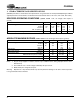
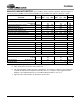
POWER AND THERMAL CHARACTERISTICS
Notes: 11. Current consumption increases with increasing FS and increasing MCLK. Variance between speed
modesissmall.
12. VD current consumption increases (ID normal and ID_pdn) when VD - VL > 1.5V. When VD - VL = 1.7V,
I
D
typically increases by 2 mA and when VD - VL = 2V, I
D
typically increases by 12 mA.
13. Power down mode is defined as RST
pin = Low with clocks running.
DIGITAL CHARACTERISTICS (AGND, DGND = 0V, all voltages with respect to ground.)
Parameters Symbol Min Typ Max Units
Power Supplies
Power Supply Current normal operation, V
A
=V
D
=V
L
=5V
(Note 11, Note 12) BRM
power-down state (all supplies) (Note 13)
BRM
I
A
I
D
I
L
I
A
I
D
I
L
-
-
-
-
-
-
35
78
0.3
0.2
0.4
0.2
42
105
2
1
15
0.5
mA
mA
mA
mA
mA
mA
Power Dissipation (Note 11)
V
A
=V
D
=V
L
= 5V normal operation
power-down (Note 13)
-
-
567
4
715
12.5
mW
mW
Package Thermal Resistance TSSOP (-KS) θ
JA
θ
JC
-
-
56
37
-
-
°C/Watt
°C/Watt
Power Supply Rejection Ratio (1 kHz, 10 mV
rms
)PSRR - 50 - dB
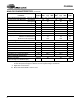
Parameter Symbol Min Max Units
High-level Input Voltage VL=5V
Low-level Input Voltage
V
IH
V
IL
0.7 x VL
-
-
0.3 x VL
V
V
High-level Input Voltage VL=3.3V
Low-level Input Voltage
V
IH
V
IL
2.2
-
-
1.0
V
V
High-level Output Voltage at
VL = 5V I
0
=-2.0mA
I
0
= -100 µA
VL = 3.3V I
0
=-2.0mA
V
OH
V
OH
V
OH
VL - 1.0
VL - 0.7
2.3
-
-
-
V
V
V
Low-level Output Voltage at
VL = 5V I
0
=2.0mA
I
0
= 100 µA
VL = 3.3V I
0
=-2.0mA
V
OL
V
OL
V
OL
-
-
-
0.4
0.2
0.4
V
V
V
Input Leakage Current (Digital Inputs) - 10 µA
Output Leakage Current (High-Impedance Digital Outputs) - 10 µA