
User Manual


CS4228A
27
LRCK 6 Left/Right Clock (Bidirectional) - The Left/Right clock determines which channel is cur-
rently being input or output on the serial audio data output, SDOUT. In Master mode, LRCK
is an output, in Slave Mode, LRCK is an input whose frequency must be equal to Fs and
synchronous to the Master clock.
Audio samples in Left/Right pairs represent simultaneously sampled analog inputs whereas
Right/Left pairs will exhibit a one sample period difference. The required relationship
between the Left/Right clock, serial clock and serial data is defined by the Serial Port Mode
register. The options are detailed in Figures 10, 11, 12 and 13
DGND 7 Digital Ground (Input) - Digital Ground Reference.
VD 8 Digital Power (Input) - Digital Power Supply.
VL 9 Digital Interface Power (Input) - Digital interface power supply. All digital output voltages
and input threshholds scale with VL.
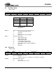
MCLK 10 Master Clock (Input) - The master clock frequency must be either 128x, 256x, 384x or
512x the input sample rate in Base Rate Mode (BRM) and either 64x, 128x, 192x, or 256x
the input sample rate in High Rate Mode (HRM). Table 3 illustrates several standard audio
sample rates and the required master clock frequencies. The MCLK/Fs ratio is set by the
CI1:0 bits in the CODEC Clock Mode register.
SCL/CCLK 11 Serial Control Interface Clock (Input) - Clocks the serial control data into or out of
SDA/CDIN.
SDA/CDIN 12 Serial Control Data I/O (Bidirectional/Input)-InI
2
C mode, SDA is a bidirectional control
port data line. A pull up resistor must be provided for proper open drain output operation. In
SPI mode, CDIN is the control port data input line. The state of the SDOUT pin during reset
is used to set the control port mode.
ADO/CS
13 AddressBit0/ChipSelect(Input) - In I
2
C mode, AD0 is the LSB of the chip address. In
SPI mode, CS
is used as a enable for the control port interface.
RST
14 Reset (Input) - When low, the device enters a low power mode and all internal registers
are reset to the default settings, including the control port. The control port can not be
accessed when reset is low.
When high, the control port and the CODEC become operational.
MUTEC 15 Mute Control (Output) - The Mute Control pin goes low during the following conditions:
power-up initialization, power-down, reset, no master clock present, or if the master clock to
left/right clock frequency ratio is incorrect. The Mute Control pin can also be user controlled
by the MUTEC bit in the DAC Mute2 Control register. Mute Control can be automatically as-
serted when 512 consecutive zeros are detected on all six DAC inputs, and automatically
deasserted when a single non-zero value is sent to any of the six DACs. The mute on zero
function is control
led by the MUTCZ bit in the DAC Mute2 Control register. The MUTEC pin
is intended to be used as a control for an external mute circuit to achieve a very low noise
floor during periods when no audio is present on the DAC outputs, and to prevent the clicks
and pops that can occur in any single supply system. Use of the Mute Control pin is not man-
da
tory but recommended.
Sample
Rate
(kHz)
MCLK (MHz)
HRM BRM
64x 128x 192x 256x 128x 256x 384x 512x
32 - - - - 4.0960 8.1920 12.2880 16.3840
44.1 - - - - 5.6448 11.2896 16.9344 22.5792
48 - - - - 6.1440 12.2880 18.4320 24.5760
64 4.0960 8.1920 12.2880 16.3840 - - - -
88.2 5.6448 11.2896 16.9344 22.5792 - - - -
96 6.1440 12.2880 18.4320 24.5760 - - - -
Table 3. Common Master Clock Frequencies