
User Manual


CS4228A
26
6. PIN DESCRIPTION
SDIN1, SDIN2,
SDIN3
1, 2, 3 Serial Audio Data In (Input) - Two's complement MSB-first serial audio data is input on this
pin. The data is clocked into SDIN1, SDIN2, SDIN3 via the serial clock and the channel is
determined by the Left/Right clock. The required relationship between the Left/Right clock,
serial clock and serial data is defined by the Serial Mode Register. The options are detailed
in Figures 10, 11, 12, and 13.
SDOUT 4 Serial Audio Data Out (Output) - Two's complement MSB-first serial data is output on this
pin. The data is clocked out of SDOUT via the serial clock and the channel is determined by
the Left/Right clock. The required relationship between the Left/Right clock, serial clock and
serial data is defined by the Serial Mode Register. The options are detailed in Figures 10,
11, 12 and 13.
The state of the SDOUT pin during reset is used to set the Control Port Mode (I
2
C or SPI).
When RST
is low, SDOUT is configured as an input, and the rising edge of RST latches the
state of the pin. A weak internal pull up is present such that a resistive load less than 47 kΩ
will pull the pin low, and the control port mode is I
2
C. When the resistive load on SDOUT is
greater than 47 kΩ during reset, the control port mode is SPI.
SCLK 5 Serial Clock (Bidirectional) - Clocks serial data into the SDIN1, SDIN2, and SDIN3 pins,
and out of the SDOUT pin. The pin is an output in master mode, and an input in slave
mode.
In master mode, SCLK is configured as an output. MCLK is divided internally to generate
SCLK at the desired multiple of the sample rate.
In slave mode, SCLK is configured as an input. The serial clock can be provided externally,
or the pin can be grounded and the serial clock derived internally from MCLK.
The required relationship between the Left/Right clock, serial clock and serial audio data is
defined by the Serial Port Mode register. The options are detailed in Figures 10, 11, 12
and 13.
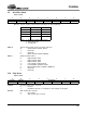
Serial Audio Data In 3 SDIN3 SUB Analog Out #6,Subwoofer
Serial Audio Data In 2 SDIN2 CENTER Analog Out #5, Center
Serial Audio Data In 1 SDIN1 SR Analog Out #4, Surround Righ
t
Serial Audio Data Out SDOUT SL Analog Out #3, Surround Left
Serial Clock SCLK FR Analog Out #2, Front Right
Left/Right Clock LRCK FL Analog Out #1, Front Left
Digital Ground DGND AGND Analog Ground
Digital Power VD VA Analog Power
Digital Interface Power VL AINL+ Left Channel Analog Input+
Master Clock MCLK AINL- Left Channel Analog Input-
SCL/CCLK SCL/CCLK FILT Internal Voltage Filter
SDA/CDIN SDA/CDIN AINR- Right Channel Analog Input-
AD0/CS
AD0/CS AINR+ Right Channel Analog Input+
Reset RST
MUTEC Mute Control
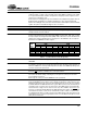
1
2
3
4
5
6
7
8
9
10
11
12
5
1
2
6
24
23
22
21
20
19
18
17
16
1514
13
25
26
27
28