
User Manual


CS4228A
22
5. REGISTER DESCRIPTIONS
All registers are read/write except for Chip Status, which is read only. See the following bit definition tables
for bit assignment information. The default state of each bit after a power-up sequence or reset is listed
in the tables underneath each bit’s label. Default values are also marked in the text with an asterisk.
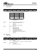
5.1 Memory Address Pointer (MAP)
Not a register
INCR memory address pointer auto increment control
0 - MAP is not incremented automatically.
*1 - internal MAP is automatically incremented after each read or write.
MAP4:0 Memory address pointer (MAP). Sets the register address that will be read or written by the con-
trol port.
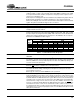
5.2 CODEC Clock Mode
Address 0x01
HRM Sets the sample rate mode for the ADCs and DACs
*0- BaseRateMode(BRM)supportssampleratesupto50kHz
1 - High Rate Mode (HRM) supports sample rates up to 100 kHz. Typically used for
96 kHz sample rate.
CI1:0 Specifies the ratio of MCLK to the sample rate of the ADCs and DACs (Fs)
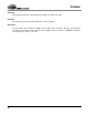
5.3 Chip Control
Address 0x02
DIGPDN
Power down the digital portions of the CODEC
0 - Digital power down.
*1 - Normal operation
ADCPDN Power down the analog section of the ADC
*0 - Normal
1 - ADC power down.
76543210
INCR RESERVED MAP4 MAP3 MAP2 MAP1 MAP0
10000001
76543210
HRM RESERVED CI1 CI0 RESERVED
00000100
CI1:0 BRM (Fs) HRM (Fs)
0 128 64
*1 256 128
2384192
3512256
7 6543210
DIGPDN
RESERVED ADCPDN DACPDN56 DACPDN34 DACPDN12 RESERVED
1 0000000