
User Manual


CS4228A
11
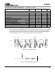
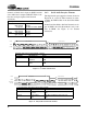
SWITCHING CHARACTERISTICS - CONTROL PORT (Inputs: Logic 0 = 0V, Logic 1 = VL)
Notes: 20. Data must be held for sufficient time to bridge the 300 ns transition time of SCL.
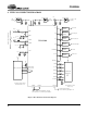
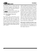
21. Pin 11 (SCL/CCLK) of the CS4228A does not have sufficient hysteresis to enable the use of standard
two-wire mode configurations with a resistor pull-up. This issue can be worked around by placing a
Schmitt Trigger buffer, for example a 74VHC14, on the SCL line just prior to the CS4228A. See Figure 5.
This will not affect the operation of the bus in either mode, as pin 6 is an input only.
Parameter Symbol Min Max Units
I
2
C Mode (SDOUT < 47 kΩ to ground)
SCL Clock Frequency f
scl
-100kHz
Bus Free Time Between Transmissions t
buf
4.7 µs
Start Condition Hold Time (prior to first clock pulse) t
hdst
4.0 µs
Clock Low Time t
low
4.7 µs
Clock High Time t
high
4.0 µs
Setup Time for Repeated Start Condition t
sust
4.7 µs
SDA Hold Time from SCL Falling (Note 20) t
hdd
0 µs
SDA Setup Time to SCL Rising t
sud
250 ns
Rise Time of Both SDA and SCL Lines (Note 21) t
r
30 ns
Fall Time of Both SDA and SCL Lines t
f
300 ns
Setup Time for Stop Condition t
susp
4.7 µs
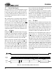
t
buf
t
hdst
t
hdst
t
low
t
r
t
f
t
hdd
t
high
t
sud
t
sust
t
susp
Stop S ta rt
Start
Stop
Repeated
SDA
SCL
Figure 4. I
2
CControlPortTiming
Figure 5. I
2
CModeSCLBufferExample
Pin 11
V+
SCL