
User Manual


CS4228A
10
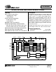
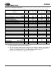
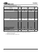
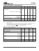
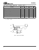
SWITCHING CHARACTERISTICS - CONTROL PORT (Inputs: Logic 0 = 0V, Logic 1 = VL)
Notes: 18. Data must be held for sufficient time to bridge the transition time of CCLK.
19. For F
SCK
<1MHz
Parameter Symbol Min Max Units
SPI Mode (SDOUT > 47 kΩ to GND)
CCLK Clock Frequency f
sck
-6MHz
CS
High Time Between Transmissions t
csh
1.0 µs
CS
Falling to CCLK Edge t
css
20 ns
CCLK Low Time t
scl
66 ns
CCLK High Time t
sch
66 ns
CDIN to CCLK Rising Setup Time t
dsu
40 ns
CCLK Rising to DATA Hold Time (Note 18) t
dh
15 ns
Rise Time of CCLK and CDIN (Note 19) t
r2
30 ns
Fall Time of CCLK and CDIN (Note 19) t
f2
100 ns
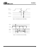
t
r2
t
f2
t
dsu
t
dh
t
sch
t
scl
CS
CCLK
CDIN
t
css
t
csh
Figure 3. SPI Control Port Timing