CS4228A 24-Bit, 96 kHz Surround Sound Codec Features Description ! Six The CS4228A codec provides two analog-to-digital and six digital-to-analog Delta-Sigma converters, along with volume controls, in a compact 28-pin SSOP device.
CS4228A TABLE OF CONTENTS 1. CHARACTERISTICS AND SPECIFICATIONS ........................................................................ 4 SPECIFIED OPERATING CONDITIONS ................................................................................. 4 ABSOLUTE MAXIMUM RATINGS ........................................................................................... 4 ANALOG CHARACTERISTICS ................................................................................................
CS4228A 4. 5. 6. 7. 8. 3.7 Control Port Signals ......................................................................................................... 18 3.7.1 SPI Mode ............................................................................................................ 18 3.7.2 I2C Mode ............................................................................................................ 18 3.8 Control Port Bit Definitions .................................................................
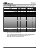
CS4228A 1. CHARACTERISTICS AND SPECIFICATIONS (Min/Max performance characteristics and specifications are guaranteed over the Specified Operating Conditions. Typical performance characteristics are derived from measurements taken at TA = 25°C, VA = 5.0V, VD = 5.0V) SPECIFIED OPERATING CONDITIONS ((AGND, DGND = 0V; all voltages with respect to ground.) Parameter DC Power Supply Symbol Min Typ Max Units Digital Analog Interface VD - VL (Note 12) VD VA VL 4.75 4.75 3.0* - 5.0 5.0 - 5.25 5.25 5.
CS4228A ANALOG CHARACTERISTICS (Test conditions (unless otherwise specified): Input test signal is a 997 Hz sine wave at 0 dBFS; measurement bandwidth is 10 Hz to 20 kHz; test load RL = 10 kΩ, CL = 15 pF) Base Rate Mode Parameter Symbol Min Typ Max High Rate Mode Min Typ Max Units Analog Input Characteristics - Minimum gain setting (0 dB) Differential Input; unless otherwise specified.
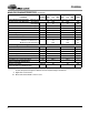
CS4228A ANALOG CHARACTERISTICS (Continued) Base Rate Mode Parameter Symbol Min Typ Max High Rate Mode Min Typ Max Units Analog Output Characteristics - Minimum Attenuation, 10 kΩ, 10 pF load; unless otherwise specified. Dynamic Range, -60 dBFS input (A weighted) (unweighted) 93 - 100 97 - 93 - 100 97 - dB dB Total Harmonic Distortion + Noise (unweighted) THD+N - -90 -83 - -90 -83 dB Interchannel Isolation - 95 - - 95 - dB Interchannel Gain Mismatch - 0.1 - - 0.
CS4228A POWER AND THERMAL CHARACTERISTICS Parameters Power Supplies Power Supply Current (Note 11, Note 12) normal operation, VA= VD =VL =5V BRM power-down state (all supplies) (Note 13) BRM Power Dissipation VA= VD = VL = 5V Package Thermal Resistance (Note 11) normal operation power-down (Note 13) TSSOP (-KS) Power Supply Rejection Ratio (1 kHz, 10 mVrms) Symbol Min Typ Max Units IA ID IL - 35 78 0.3 42 105 2 mA mA mA IA ID IL - 0.2 0.4 0.2 1 15 0.5 mA mA mA - 567 4 715 12.
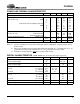
CS4228A SWITCHING CHARACTERISTICS (Inputs: Logic 0 = 0V, Logic 1 = VL) Parameter Symbol Min Typ Max Units Fs 30 60 - 50 100 kHz kHz 3.84 - 25.
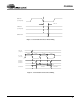
CS4228A S C LK ( o u tp u t) t m s lr LR C K ( o u tp u t) S D O U T Figure 1. Serial Audio Port Master Mode Timing LR C K ( in p u t) t lr c k d t lr c k s t sckh tsckl SC LK ( in p u t) S D IN 1 S D IN 2 S D IN 3 t lr p d SD O U T td s td h M S B td p d M S B -1 Figure 2.
CS4228A SWITCHING CHARACTERISTICS - CONTROL PORT (Inputs: Logic 0 = 0V, Logic 1 = VL) Parameter Symbol Min Max Units CCLK Clock Frequency fsck - 6 MHz CS High Time Between Transmissions tcsh 1.
CS4228A SWITCHING CHARACTERISTICS - CONTROL PORT (Inputs: Logic 0 = 0V, Logic 1 = VL) Parameter Symbol Min Max Units SCL Clock Frequency fscl - 100 kHz Bus Free Time Between Transmissions tbuf 4.7 µs Start Condition Hold Time (prior to first clock pulse) thdst 4.0 µs Clock Low Time tlow 4.7 µs Clock High Time thigh 4.0 µs Setup Time for Repeated Start Condition tsust 4.
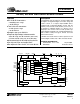
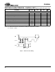
CS4228A 2. TYPICAL CONNECTION DIAGRAM +5V S upply VL Ferrite B ead Ferrite B ead + 1 µF 0.1 µ F 1 µF + 0.1 µ F 21 VA +5 V S upply 8 Ferrite B ead + 0.1 µ F 9 VL VD AN AL O G FILTE R Front Left 23 AN AL O G FILTE R Front Right 24 AN AL O G FILTE R Surround Left 25 26 AN AL O G FILTE R Surround Right AN AL O G FILTE R Center 27 AN AL O G FILTE R Subwoofer 28 FL 22 µ F 150 Ω + F ro m A n alog Inp ut S tage 19 A IN LFR 2.2 nf 100 µ F 22 µ F + + 20 A IN L+ 0.
CS4228A 3. FUNCTIONAL DESCRIPTION 3.1 positive or negative input as long as the unused input is connected to ground through capacitors as shown. When operated with single-ended inputs, distortion will increase at input levels higher than -1 dBFS. Figure 7 shows an example of a differential input circuit. Overview The CS4228A is a 24-bit audio codec comprised of 2 analog-to-digital converters (ADC) and 6 digitalto-analog converters (DAC), all implemented using single-bit delta-sigma techniques.
CS4228A The high pass filters can be disabled by setting the HPF bit in the ADC Control register. When asserted, any DC present at the analog inputs will be represented in the ADC outputs. The high pass filter may also be “frozen” using the HPFZ bit in the ADC Control register. In this condition, it will remember the DC offset present at the ADC inputs at the moment the HPFZ bit was asserted, and will continue to remove this DC level from the ADC outputs.
CS4228A returns to the attenuation level set in the Digital Volume Control register. The attenuation is ramped up and down at the rate specified by the RMP1:0 bits. is determined by the CI1:0 bits in the CODEC Clock Mode register. To achieve complete digital attenuation of an incoming signal, Hard Mute controls are provided. When asserted, Hard Mute will send zero data to a corresponding pair of DACs.
CS4228A 3.6.2 channels of DAC data is input on SDIN1 and the stereo ADC data is output on SDOUT. Table 1 outlines the serial port input to DAC channel allocations. DAC Inputs SDIN1 left channel right channel single line SDIN2 left channel right channel SDIN3 left channel right channel Serial Audio Interface Formats The digital audio port supports 6 formats, shown in Figure 10, 11, 12 and 13. These formats are selected using the DDF2:0 bits in the Serial Port Mode register.
CS4228A LRCK Right Channel Left Channel SCLK SDINx 15 14 13 12 11 10 9 8 7 6 5 4 3 2 1 0 15 14 13 12 11 10 9 8 7 6 5 4 3 2 1 0 Right Justified Mode, Data Valid on Rising Edge of SCLK Bits/Sample SCLK Rate(s) Notes 16 32, 48, 64, 128 Fs 32, 64 Fs BRM, 48 Fs available in slave mode only HRM 20 48, 64, 128 Fs 64 Fs BRM, 48 Fs available in slave mode only HRM 24 48, 64, 128 Fs 64 Fs BRM, 48 Fs available in slave mode only HRM Figure 12.
CS4228A 3.7 Control Port Signals bytes contain the data which will be placed into the registers designated by the MAP. Internal registers are accessed through the control port. The control port may be operated asynchronously with respect to audio sample rate. However, to avoid potential interference problems, the control port pins should remain static if no register access is required. The CS4228A has a MAP auto increment capability, enabled by the INCR bit in the MAP register.
CS4228A 0 1 2 3 4 5 6 7 8 9 10 11 12 13 14 15 16 17 18 24 25 26 27 28 19 SCL CHIP ADDRESS (WRITE) 0 SDA 0 1 0 0 0 MAP BYTE AD0 0 6 INCR 5 4 3 2 1 0 ACK 7 6 DATA +n DATA +1 DATA 1 0 ACK 7 6 1 0 7 6 1 0 ACK ACK STOP START Figure 15.
CS4228A The CS4228A will enter a stand-by mode if the master clock source stops for approximately 10 µs or if the number of MCLK cycles per LRCK period varies by more than 32. Should this occur, the control registers retain their settings. AGND and DGND pins should both be tied to a solid ground plane surrounding the CS4228A. The system analog and digital ground planes should not be separated under normal circumstances. A solid ground plane underneath the part is recommended.
CS4228A 4.
CS4228A 5. REGISTER DESCRIPTIONS All registers are read/write except for Chip Status, which is read only. See the following bit definition tables for bit assignment information. The default state of each bit after a power-up sequence or reset is listed in the tables underneath each bit’s label. Default values are also marked in the text with an asterisk. 5.
CS4228A DACPDN12 Power down the analog section of DAC 1 and 2 *0 Normal 1Power down DAC 1 and 2. DACPDN34 Power down the analog section of DAC 3 and 4 *0 Normal 1Power down DAC 3 and 4. DACPDN56 Power down the analog section of DAC 5 and 6 *0 Normal 1Power down DAC 5 and 6. 5.4 ADC Control Address 0x03 7 MUTL 0 6 MUTR 0 5 HPF 0 4 HPFZ 0 3 2 1 0 0 0 RESERVED 0 0 MUTL, MUTR ADC left and right channel mute control *0 Normal 1Selected ADC output muted HPF ADC DC offset removal.
CS4228A 5.6 DAC Mute2 Control Address 0x05 7 MUTEC 1 6 MUTCZ 0 5 4 3 HMUTE56 0 RESERVED 0 0 2 HMUTE34 0 1 HMUTE12 0 0 RESERVED 0 MUTEC Controls the MUTEC pin 0Normal operation *1 MUTEC pin asserted low MUTCZ Automatically asserts the MUTEC pin on consecutive zeros. When enabled, 512 consecutive zeros on all six DAC inputs will cause the MUTEC pin to be asserted low. A single non-zero value on any DAC input will cause the MUTEC pin to deassert.
CS4228A 5.9 Serial Port Mode Address 0x0D 7 DCK1 1 6 DCK0 0 DCK1:0 5 DMS1 0 4 DMS0 0 3 RESERVED 0 2 DDF2 1 1 DDF1 0 0 DFF0 0 2 1 0 0 0 0 Sets the number of Serial Clocks (SCLK) per Fs period (LRCLK) DCK1:0 BRM (Fs) HRM (Fs) 0 32 (1) (3) 1 48 (2) (3) 2 *64 32 (1) 3 128 64 Notes: 1. All formats will default to 16 bits 2. Slave mode only 3.
CS4228A 6.
CS4228A LRCK 6 Left/Right Clock (Bidirectional) - The Left/Right clock determines which channel is currently being input or output on the serial audio data output, SDOUT. In Master mode, LRCK is an output, in Slave Mode, LRCK is an input whose frequency must be equal to Fs and synchronous to the Master clock. Audio samples in Left/Right pairs represent simultaneously sampled analog inputs whereas Right/Left pairs will exhibit a one sample period difference.
CS4228A AINR+, AINR-, AINL+, AINL- 16, 17, 19, 20 Differential Analog Inputs (Input) - The analog signal inputs are presented differentially to the modulators via the AINR+/- and AINL+/- pins. The + and - input signals are 180° out of phase resulting in a nominal differential input voltage of twice the input pin voltage. These pins are biased to the internal reference voltage. A passive anti-aliasing filter is required for best performance, as shown in Figure 6.
CS4228A 7. PARAMETER DEFINITIONS Dynamic Range The ratio of the full scale RMS value of the signal to the RMS sum of all other spectral components over the specified bandwidth. Dynamic range is a signal-to-noise measurement over the specified bandwidth made with a -60 dBFS signal. 60 dB is then added to the resulting measurement to refer the measurement to full scale. This technique ensures that the distortion components are below the noise level and do not effect the measurement.
CS4228A Gain Error The deviation from the nominal full scale output for a full scale input. Gain Drift The change in gain value with temperature. Units in ppm/°C. Offset Error For the ADCs, the deviation in LSBs of the output from mid-scale with the selected input grounded. For the DACs, the deviation of the output from zero (relative to CMOUT) with midscale input code. Units are in Volts.
CS4228A 8. PACKAGE DIMENSIONS 28L SSOP PACKAGE DRAWING N D E11 A2 E e b2 SIDE VIEW A ∝ A1 L END VIEW SEATING PLANE 1 2 3 TOP VIEW DIM A A1 A2 b D E E1 e L ∝ MIN -0.002 0.064 0.009 0.390 0.291 0.197 0.022 0.025 0° INCHES NOM -0.006 0.069 -0.4015 0.307 0.209 0.026 0.0354 4° MAX 0.084 0.010 0.074 0.015 0.413 0.323 0.220 0.030 0.041 8° MIN -0.05 1.62 0.22 9.90 7.40 5.00 0.55 0.63 0° MILLIMETERS NOM -0.15 1.75 -10.20 7.80 5.30 0.65 0.90 4° NOTE MAX 2.13 0.25 1.88 0.38 10.50 8.20 5.60 0.