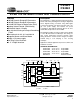
CS4223 CS4224 24-Bit 105 dB Audio Codec with Volume Control Features Description 105 dB Dynamic Range A/D Converters 105 dB Dynamic Range D/A Converters 110 dB DAC Signal-to-Noise Ratio (EIAJ) Analog Volume Control (CS4224 only) Differential Inputs / Outputs On-chip Anti-aliasing and Output Smoothing The CS4223/4 is a highly integrated, high performance, 24-bit, audio codec providing stereo analog-to-digital and stereo digital-to-analog converters using delta-sigma conversion techniques.
CS4223 CS4224 TABLE OF CONTENTS 1. CHARACTERISTICS AND SPECIFICATIONS ........................................................................ 4 SPECIFIED OPERATING CONDITIONS ................................................................................. 4 ABSOLUTE MAXIMUM RATINGS ........................................................................................... 4 ANALOG CHARACTERISTICS ................................................................................................
CS4223 CS4224 5.5.3 Serial Data Output Format (DOF).................................................................................. 17 5.5.4 Serial Data Input Format (DIF) ...................................................................................... 17 5.6 Converter Status Report (Read Only) (address 06h) ....................................................... 18 5.6.1 Left and Right Channel Acceptance Bit (ACCR-ACCL) ................................................ 18 5.6.
CS4223 CS4224 LIST OF TABLES Table 1. Example Volume Settings ............................................................................................... 16 Table 2. Common Clock Frequencies ........................................................................................... 19 Table 3. Digital Interface Format - DIF1 and DIF0 ....................................................................... 20 Table 4. De-emphasis Control.....................................................................
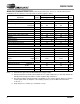
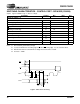
CS4223 CS4224 1. CHARACTERISTICS AND SPECIFICATIONS (All Min/Max characteristics and specifications are guaranteed over the Specified Operating Conditions. Typical performance characteristics and specifications are derived from measurements taken at nominal supply voltages and TA = 25°C.) SPECIFIED OPERATING CONDITIONS (AGND, DGND = 0 V, all voltages with respect to 0 V.) Parameter Symbol Min Nom Max Unit Digital Analog Digital | VA - VD | VD VA VL 4.75 4.75 2.7 - 5.0 5.0 5.0 - 5.25 5.25 5.25 0.
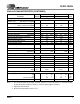
CS4223 CS4224 ANALOG CHARACTERISTICS (Full Scale Input Sine wave, 997 Hz; Fs = 48 kHz; Measurement Bandwidth is 20 Hz to 20 kHz; Local components as shown in Figures 4 and 5.) CS4223/4 - KS Parameter CS4223/4 - BS/ - DS Symbol Min Typ Max Min Typ Max Unit THD - 0.0014 - - 0.0014 - % 98 95 105 102 - 95 92 105 102 - dB dB - -97 -90 - -97 -87 dB - 90 - - 90 - dB - - 0.1 - - 0.
CS4223 CS4224 ANALOG CHARACTERISTICS (CONTINUED) CS4223/4 - KS Parameter Symbol Min Typ CS4223/4 - BS/ - DS Max Min Typ Max Unit Analog Output Characteristics - Minimum Attenuation, 10 kΩ, 100 pF load; unless otherwise specified. Signal-to-Noise, Idle-Channel Noise (CS4224 only) DAC muted, A-weighted 102 110 - 97 110 - dB Dynamic Range 100 97 105 102 - 95 92 105 102 - dB dB THD - 0.0014 - - 0.
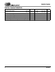
CS4223 CS4224 DIGITAL CHARACTERISTICS Parameter Symbol Min Max Unit VIH VIH 2.8 2.0 VL + 0.3 VL + 0.3 V V Low-level Input Voltage VIL -0.3 0.8 V High-level Output Voltage at IO = -2.0 mA VOH VL - 1.0 - V Low-level Output Voltage at IO = 2.0 mA VOL - 0.
CS4223 CS4224 SWITCHING CHARACTERISTICS (Outputs loaded with 30 pF) Parameter Symbol Audio ADC’s and DAC’s Sample Rate XTI Frequency Min Typ Max Fs XTI = 256, 384, or 512 Fs Unit 4 - 50 kHz 1.
CS4223 CS4224 SWITCHING CHARACTERISTICS - CONTROL PORT - SPI MODE (CS4224) (Inputs: Logic 0 = DGND, Logic 1 = VD; CL = 30 pF) Parameter Symbol Min Max Unit fsck - 6 MHz SPI Mode (SPI/I2C = 0) CCLK Clock Frequency RST rising edge to CS falling (Note 11) tsrs 41 - µs CCLK edge to CS falling (Note 12) tspi 500 - ns CS High Time between transmissions tcsh 1.
CS4223 CS4224 SWITCHING CHARACTERISTICS - CONTROL PORT - I2C MODE (CS4224) (Inputs: Logic 0 = DGND, Logic 1 = VD; CL = 30 pF) Parameter Symbol Min Max Unit fscl - 100 kHz tirs 50 - µs Bus Free Time between transmissions tbuf 4.7 - µs Start Condition Hold Time (prior to first clock pulse) thdst 4.0 - µs Clock Low Time tlow 4.7 - µs Clock High Time thigh 4.0 - µs Setup time for repeated Start Condition tsust 4.
CS4223 CS4224 2. TYPICAL CONNECTION DIAGRAM — CS4223 Ferrite Bead +5V Supply 2Ω +2.7 - 5V + 1 µF 150Ω 150Ω 150Ω 0.1 µF 0.1 µF + 1 µF 21 VA 20 AINL+ 2.2 nF 19 6 VD VL AOUTL+ AOUTL- AINL- AOUTR+ AOUTR- 17 AINR+ DEM1 2.2 nF 150Ω 16 DEM0 AINR- CS4223 XTI 0.
CS4223 CS4224 3. TYPICAL CONNECTION DIAGRAM — CS4224 Ferrite Bead +5V Supply 2Ω +2.7 - 5V + 1 µF 150Ω 150Ω 150Ω 150Ω 0.1 µF 0.1 µF + 1 µF 21 VA 20 AINL+ 2.2 nF 19 AOUTL+ AOUTLAOUTR+ AOUTR- AINL- 17 6 VD VL 0.1 µF + 1 µF 13 25 26 Analog Filter 24 23 Analog Filter AINR+ 2.
CS4223 CS4224 4.
CS4223 CS4224 5. REGISTER DESCRIPTIONS - CS4224 Note: All registers are read/write in I2C mode and write-only in SPI mode, unless otherwise noted. 5.1 ADC Control (address 01h) 7 PDN 0 5.1.1 6 HPDR 0 5 HPDL 0 4 ADMR 0 3 ADML 0 2 CAL 0 1 CALP 0 0 CLKE 0 POWER DOWN ADC (PDN) Default = 0 0 - Disabled 1 - Enabled Function: The ADC will enter a low-power state when this function is enabled. 5.1.
CS4223 CS4224 5.1.6 CLOCKING ERROR (CLKE) (READ ONLY) Default = 0 0 - No error 1 - Error 5.2 DAC Control (address 02h) 7 Reserved 0 5.2.1 6 MUTC 0 5 MUTR 0 4 MUTL 0 3 SOFT 0 2 Reserved 0 1 RMP1 0 0 RMP0 0 MUTE ON CONSECUTIVE ZEROS (MUTC) Default = 0 0 - Disabled 1 - Enabled Function: The DAC output will mute following the reception of 512 consecutive audio samples of static 0 or -1 when this function is enabled. A single sample of non-static data will release the mute.
CS4223 CS4224 5.2.4 SOFT RAMP STEP RATE (RMP) Default = 00 00 - 1 step per 8 LRCK's 01 - 1 step per 4 LRCK's 10 - 1 step per 16 LRCK's 11 - 1 step per 32 LRCK's Function: The rate of change for the Soft Ramp function is adjustable through the RMP bits. 5.3 Left Channel Output Attenuator Level (address 03h) 5.4 Right Channel Output Attenuator Level (address 04h) 7 ATT7 0 5.4.
CS4223 CS4224 5.5 DSP Port Mode (address 05h) 7 6 DEM1 0 Reserved 0 5.5.1 5 DEM0 0 4 DSCK 0 3 DOF1 0 2 DOF0 0 1 DIF1 0 0 DIF0 0 DE-EMPHASIS CONTROL (DEM) Default = 00 00 - 44.1 kHz de-emphasis setting 01 - 48 kHz de-emphasis setting 10 - 32 kHz de-emphasis setting 11 - De-emphasis disabled Function: Selects the appropriate digital filter to maintain the standard 15 µs/50 µs digital de-emphasis filter response at 32, 44.1 or 48 kHz sample rates, see Figure 15. 5.5.
CS4223 CS4224 5.6 Converter Status Report (Read Only) (address 06h) 7 ACCR 0 5.6.1 6 ACCL 0 5 LVR2 0 4 LVR1 0 3 LVR0 0 2 LVL2 0 1 LVL2 0 0 LVL0 0 LEFT AND RIGHT CHANNEL ACCEPTANCE BIT (ACCR-ACCL) Default = 0 0 - Requested setting valid 1 - New setting loaded Function: The ACCR and ACCL bits indicate when a change in the Output Attenuator Level has occurred for the left and right channels, respectively. The value will be high when a new setting is loaded into the Output Attenuator Level registers.
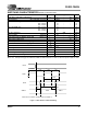
CS4223 CS4224 6. PIN DESCRIPTIONS — CS4223 CS4223 NC XTI, XTO NC 1 28 NC XTO 2 27 RST XTI 3 26 AOUTL- LRCK 4 25 AOUTL+ SCLK 5 24 AOUTR+ VD 6 23 AOUTR- DGND 7 22 AGND SDOUT 8 21 VA SDIN 9 20 AINL+ DIF1 10 19 AINL- DIF0 11 18 DEM1 DEM0 12 17 AINR+ VL 13 16 AINR- NC 14 15 NC 1,14,15, 28 No Connect - These pins are not connected internally and should be tied to DGND to minimize noise coupling.
CS4223 CS4224 SDIN DIF0, DIF1 9 Serial Data Input (Input) - Two's complement MSB-first serial data is input on this pin. The required relationship between the left/right clock, serial clock and serial data is defined by the DIF1-0 pins. The options are detailed in Figures 8 - 11. 10,11 Digital Interface Format (Input) - The required relationship between the left/right clock, serial clock and serial data is defined by the Digital Interface Format. The options are detailed in Figures 8 - 11.
CS4223 CS4224 7. PIN DESCRIPTIONS — CS4224 CS4224 NC XTI, XTO NC 1 28 NC XTO 2 27 RST XTI 3 26 AOUTL- LRCK 4 25 AOUTL+ SCLK 5 24 AOUTR+ VD 6 23 AOUTR- DGND 7 22 AGND SDOUT 8 21 VA SDIN 9 20 AINL+ SCL/CCLK 10 19 AINL- SDA/CDIN 11 18 I2C/SPI AD0/CS 12 17 AINR+ VL 13 16 AINR- NC 14 15 NC 1,14,15, 28 No Connect - These pins are not connected internally and should be tied to DGND to minimize noise coupling.
CS4223 CS4224 SDOUT 8 Serial Data Output (Output) - Two's complement MSB-first serial data is output on this pin. The required relationship between the left/right clock, serial clock and serial data is defined by the DSP Port Mode (05h) register. The options are detailed in Figures 8 - 11. SDIN 9 Serial Data Input (Input) - Two's complement MSB-first serial data is input on this pin.
CS4223 CS4224 8. APPLICATIONS The CS4223 is a stand-alone device controlled through dedicated pins. The CS4224 is controlled with an external microcontroller using the serial control port. LRCK are outputs which are internally derived from MCLK. The device will operate in master mode when a 47 kΩ pulldown resistor is present on SDOUT at startup or after reset, see Figure 5. LRCK and SCLK are inputs to the CS4223/4 when operating in slave mode. See Figures 8-11 for the available clocking modes. 8.2 8.
CS4223 CS4224 8.8 Control Port Interface (CS4224 only) The control port is used to load all the internal settings. The operation of the control port may be completely asynchronous with the audio sample rate. However, to avoid potential interference problems, the control port pins should remain static if no operation is required. The control port has 2 modes: SPI and I2C, with the CS4224 operating as a slave device. The control port interface format is selected by the SPI/I2C pin. 8.8.
CS4223 CS4224 8.9 Memory Address Pointer (MAP) 7 INCR 0 8.9.1 6 5 4 3 Reserved Reserved Reserved Reserved 0 0 0 0 2 MAP2 0 1 MAP1 0 0 MAP0 0 AUTO-INCREMENT CONTROL (INCR) Default = 0 0 - Disabled 1 - Enabled 8.9.2 REGISTER POINTER (MAP) Default = 000 CS CCLK CHIP ADDRESS MAP 0010000 CDIN R/W DATA 00000000 00000000 00000000 LSB 00000000 00000000 MSB byte 1 MAP = Memory Address Pointer byte n Figure 6.
CS4223 CS4224 L eft C ha n n el LRC K R igh t C ha n n el SC L K SDATA MS B -1 -2 -3 -4 -5 +5 +4 +3 +2 +1 LS B MSB -1 -2 -3 -4 +5 +4 +3 +2 +1 LSB Master Slave I2S, up to 24-bit data XTI=256, 384, 512 Fs (CS4223 -256 Fsonly) LRCK = 4 to 50 kHz SCLK = 64 Fs I2S, up to 24-bit data XTI = 256, 384, 512 Fs LRCK = 4 to 50 kHz SCLK = 48,64, 128 Fs Figure 8.
CS4223 CS4224 LR CK R ig h t C h a n n e l L e ft C h a n n e l SC LK S DA TA 1 0 19 18 17 16 15 14 13 12 11 10 9 8 7 6 5 4 3 2 1 0 19 18 17 16 15 14 13 12 11 10 9 8 7 6 5 4 3 2 1 0 32 clocks Master Slave Right-justified, 20-bit data XTI=256, 384, 512Fs (CS4223-256Fsonly) LRCK = 4 to 50 kHz SCLK = 64 Fs Right-justified, 20-bit data XTI = 256, 384, 512 Fs LRCK = 4 to 50 kHz SCLK = 64 Fs Figure 11. Serial Audio Format 3 Figure 12.
CS4223 CS4224 Figure 14. 2- and 3-Pole Butterworth Filters Gain dB -10 dB F2 Frequency Figure 15. De-emphasis Curve Amplitude (dB) T2 = 15 µs DS290F1 Digital Signal 0 dB F1 Analog 0 T1 = 50 µs Noise 0 Attenuation (dB) -113.5 Figure 16.
CS4223 CS4224 9. ADC/DAC FILTER RESPONSE Figure 17. ADC Filter Response 30 Figure 18. ADC Passband Ripple Figure 19. ADC Transition Band Figure 20. DAC Filter Response Figure 21. DAC Passband Ripple Figure 22.
CS4223 CS4224 10.PARAMETER DEFINITIONS Dynamic Range The ratio of the full scale rms value of the signal to the rms sum of all other spectral components over the specified bandwidth. Dynamic range is a signal-to-noise measurement over the specified bandwidth made with a -60 dBFS signal. 60 dB is then added to the resulting measurement to refer the measurement to full scale. This technique ensures that the distortion components are below the noise level and do not affect the measurement.
CS4223 CS4224 11.PACKAGE DIMENSIONS 28L SSOP PACKAGE DRAWING N D E11 A2 E e b2 SIDE VIEW A ∝ A1 L END VIEW SEATING PLANE 1 2 3 TOP VIEW DIM A A1 A2 b D E E1 e L ∝ MIN -0.002 0.064 0.009 0.390 0.291 0.197 0.022 0.025 0° INCHES NOM -0.006 0.069 -0.4015 0.307 0.209 0.026 0.0354 4° MAX 0.084 0.010 0.074 0.015 0.413 0.323 0.220 0.030 0.041 8° MIN -0.05 1.62 0.22 9.90 7.40 5.00 0.55 0.63 0° MILLIMETERS NOM -0.15 1.75 -10.20 7.80 5.30 0.65 0.90 4° NOTE MAX 2.13 0.25 1.88 0.38 10.50 8.20 5.
• Notes •