
Manual

CS4220 CS4221
8 DS284PP3
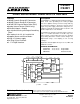
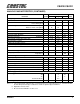
SWITCHING CHARACTERISTICS - CONTROL PORT - SPI MODE (CS4221)
(T
A
= 25° C; VA, VD = 4.75 V - 5.25 V; Inputs: Logic 0 = DGND, Logic 1 = VD; C
L
= 30 pF)
Notes: 11. Not tested but guaranteed by design.
12. t
spi
only needed before first falling edge of CS after RST rising edge. t
spi
= 0 at all other times.
13. Data must be held for sufficient time to bridge the transition time of CCLK.
14. For F
SCK
< 1 MHz.
Parameter Symbol Min Max Unit
SPI Mode (SPI/I2C = 0)
CCLK Clock Frequency f
sck
-6MHz
RST
rising edge to CS falling (Note 11) t
srs
41 - µs
CCLK edge to CS
falling (Note 12) t
spi
500 - ns
CS
High Time between transmissions t
csh
1.0 - µs
CS
falling to CCLK edge t
css
20 - ns
CCLK Low Time t
scl
66 - ns
CCLK High Time t
sch
66 - ns
CDIN to CCLK rising setup time t
dsu
40 - ns
CCLK rising to DATA hold time (Note 13) t
dh
15 - ns
Rise time of CCLK and CDIN (Note 14) t
r2
-100ns
Fall time of CCLK and CDIN (Note 14) t
f2
-100ns
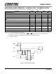
t
r2
t
f2
t
dsu
t
dh
t
sch
t
scl
CS
CCLK
CDIN
t
css
t
csh
t
spi
t
srs
RST
Figure 2. SPI Control Port Timing