
Manual

CS4220 CS4221
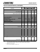
DS284PP3 7
SWITCHING CHARACTERISTICS (T
A
= 25° C; VA, VD = 4.75 V - 5.25 V; outputs loaded with
30 pF)
Notes: 10. After powering up the CS4220/1, PDN should be held low for 10 ms to allow the power supply to settle.
Parameter Symbol Min Typ Max Unit
Audio ADC’s and DAC’s Sample Rate Fs 4 - 50 kHz
XTI Frequency XTI = 256, 384, or 512 Fs 1.024 - 26 MHz
XTI Pulse Width High XTI = 512 Fs
XTI = 384 Fs
XTI = 256 Fs
13
21
31
-
-
-
-
-
-
ns
XTI Pulse Width Low XTI = 512 Fs
XTI = 384 Fs
XTI = 256 Fs
13
21
31
-
-
-
-
-
-
ns
XTI Jitter Tolerance - 500 - psRMS
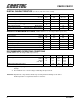
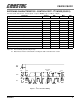
RST
Low Time (Note 10) 10 - - ms
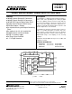
SCLK falling edge to SDOUT output valid DSCK = 0 t
dpd
-- ns
LRCK edge to MSB valid t
lrpd
- - 45 ns
SDIN setup time before SCLK rising edge DSCK = 0 t
ds
25 - - ns
SDIN hold time after SCLK rising edge DSCK = 0 t
dh
25 - - ns
SCLK Period t
sckw
--ns
SCLK High Time t
sckh
40 - - ns
SCLK Low Time t
sckl
40 - - ns
SCLK rising to LRCK edge DSCK = 0 t
lrckd
35 - - ns
LRCK edge to SCLK rising DSCK = 0 t
lrcks
40 - - ns
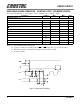
1
(384) Fs
----------------------20+
1
(128) Fs
----------------------
sckh
sckl
sckw
t
t
t
MSB MSB-1
*SCLK shown for DSCK = 0, SCLK inverted for DSCK = 1.
t
dpd
SDOUT
LRCK
SCLK*
SDIN
dh
t
ds
t
lrpd
t
lrcks
t
lrckd
t
Figure 1. Serial Audio Port Data I/O Timing