
Manual

CS4220 CS4221
18 DS284PP3
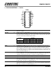
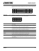
6. PIN DESCRIPTIONS — CS4220
1
2
3
4
5
6
7
821
22
23
24
25
26
27
28
NC
RST
AOUTL-
AOUTL+
AOUTR+
AOUTR-
AGND
VASDOUT
DGND
VD
SCLK
LRCK
XTI
XTO
NC
9
10
11
12 17
18
19
20
AINL+
AINL-
DEM1
AINR+DEM0
DIF0
DIF1
SDIN
13
14 15
16
AINR-
NCNC
VL
CS4220
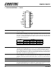
1
2
3
4
5
6
7
821
22
23
24
25
26
27
28
NC
RST
AOUTL-
AOUTL+
AOUTR+
AOUTR-
AGND
VASDOUT
DGND
VD
SCLK
LRCK
XTI
XTO
NC
9
10
11
12 17
18
19
20
AINL+
AINL-
DEM1
AINR+DEM0
DIF0
DIF1
SDIN
13
14 15
16
AINR-
NCNC
VL
CS4220
NC 1,14,15, 28 No Connect - These pins are not connected internally and should be tied to DGND to mini-
mize noise coupling.
XTI, XTO 2,3 Crystal Connections (
Input/Output
) - Input and output connections for the crystal used to
clock the CS4220. Alternatively, a clock may be input into XTI. This is the clock source for the
delta-sigma modulator and digital filters. The frequency of this clock must be either 256x, 384x,
or 512x Fs in Slave Mode and 256x in Master Mode.
LRCK 4 Left/Right Clock (
Input
) - Determines which channel is currently being input/output of the
serial audio data pins SDIN/SDOUT. The frequency of the Left/Right clock must be equal to the
input sample rate. Although the outputs for each ADC channel are transmitted at different
times, Left/Right pairs represent simultaneously sampled analog inputs. The required relation-
ship between the left/right clock, serial clock and serial data is defined by the DIF1-0 pins. The
options are detailed in Figures 8 - 11.
SCLK 5 Serial Data Clock (
Input
) - Clocks the individual bits of the serial data into the SDIN pin and
out of the SDOUT pin. The required relationship between the left/right clock, serial clock and
serial data is defined by the DIF1-0 pins. The options are detailed in Figures 8 - 11.
VD 6 Digital Power (
Input
) - Positive power supply for the digital section. Typically 5.0 VDC.
DGND 7 Digital Ground (
Input
) - Digital ground for the digital section.
SDOUT 8 Serial Data Output (
Output
) - Two’s complement MSB-first serial data is output on this pin.
The required relationship between the left/right clock, serial clock and serial data is defined by
the DIF1-0 pins. The options are detailed in Figures 8 - 11.
SDIN 9 Serial Data Input (
Input
) - Two’s complement MSB-first serial data is input on this pin. The
required relationship between the left/right clock, serial clock and serial data is defined by the
DIF1-0 pins. The options are detailed in Figures 8 - 11.
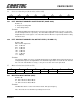
Fs (kHz) XTI (MHz)
256x 384x 512x
32 8.1920 12.2880 16.3840
44.1 11.2896 16.9344 22.5792
48 12.2880 18.4320 24.5760
Table 2. Common Clock Frequencies