
User Manual

8 DS880F4
CS4207
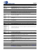
1. PIN DESCRIPTIONS
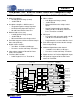
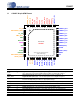
1.1 CS4207 48-pin QFN Pinout:
Pin Name QFN Pin Description
VL_IF 1
Digital Interface Signal Level (Input) - Digital supply for the GPIO, S/PDIF and Digital Mic inter-
faces. Refer to the Recommended Operating Conditions for appropriate voltages.
GPIO0/
DMIC_SDA1
2
General Purpose I/O (Input/Output) - General purpose input or output line, or
Digital Mic Data Input (Input) - The first data input line from a digital microphone.
VL_HD 3
Digital Interface Signal Level (Input) - Digital supply for the HD Audio interface. Refer to the
Recommended Operating Conditions for appropriate voltages.
DMIC_SCL 4 Digital Mic Clock (Output) - The high speed clock output to the digital microphone.
SDO 5 Serial Data Input (Input) - Serial data input stream from the HD Audio Bus.
BITCLK 6 Bit Clock (Input) - 24 MHz bit clock from the HD Audio Bus.
DGND 7 Digital Ground (Input) - Ground reference for the internal digital section.
SDI 8 Serial Data Output (Input/Output) - Serial data output stream to the HD Audio Bus.
VD 9 Digital Power (Input) - Positive power for the internal digital section.
SYNC 10 Sync Clock (Input) - 48 kHz sync clock from the HD Audio Bus.
HPREF
Thermal Pad
1413
8
7
6
5
4
3
2
1
15
16
17 18 19 20
29
30
31
32
33
34
35
36
41
424344
45
464748
37
38
3940
12
11
10
9
21 22 23 24
25
26
27
28
SPDIF_OUT1
SENSE_A
VL_IF
LINEOUT_R1+
Top-Down (Through Package) View
48-Pin QFN Package
LINEOUT_L1+
LINEOUT_L1-
LINEOUT_R2-
LINEOUT_R2+
LINEOUT_L2+
LINEOUT_L2-
VBIAS (DAC)
VCOM
VREF+ (ADC)
AGND
VA
SPDIF_IN
FLYN
FLYC
VHP_FILT-
FLYP
HPOUT_L
HPREF
HPOUT_R
VA_HP
LINEOUT_R1-
GPIO0/DMIC_SDA1
VL_HD
DMIC_SCL
SDO
BITCLK
DGND
SDI
VD
SYNC
RESET#
GPIO1/DMIC_SDA2
/SPDIF_OUT2
MICBIAS
MICIN_L-
MICIN_L+
MICIN_R+
GPIO2
GPIO3
MICIN_R-
LINEIN_L+
LINEIN_C-
LINEIN_R+
VA_REF
VHP_FILT+
HPGND