
User Manual


22 DS880F4
CS4207
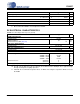
DIGITAL MICROPHONE INTERFACE CHARACTERISTICS
Test conditions: Inputs: Logic 0 = GND = 0 V, Logic 1 = VL_IF; T
A
= +25 C; C
LOAD
= 30 pF.
Notes:
12. The output clock frequency will follow the Bit Clock (BITCLK) frequency divided by 8 or 12, depending on
the sample rate of the ADC. Any deviation of the Bit Clock source from the nominal supported rates will be
directly imparted to the output clock rate by the same factor (e.g. +100 ppm offset in the frequency of BIT-
CLK will become a +100 ppm offset in DMIC_SCL). For the nominal value of T_cyc reference HDA024-A
(see Note 4 in “References” on page 147).
13. Rise and fall times are measured from 0.1 • VL_IF to 0.9 • VL_IF.
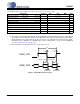
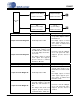
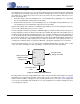
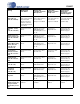
Figure 7. Digital MIC Interface Timing
Parameters Symbol Min Typ Max Units
DMIC_SCL Period (Fs
ADC
>= 44.1 kHz) (Note 12)
t
P
- 8 • T_cyc
-
ns
DMIC_SCL Period (Fs
ADC
<= 32.0 kHz) (Note 12)
t
P
- 12 • T_cyc
-
ns
DMIC_SCL Duty Cycle - 45 - 55 %
DMIC_SCL Rise Time (Note 13) t
r
- - 10 ns
DMIC_SCL Fall Time (Note 13) t
f
- - 10 ns
DMIC_SDA Setup Time Before DMIC_SCL Rising Edge t
s(SD-CLKR)
40 - - ns
DMIC_SDA Hold Time After DMIC_SCL Rising Edge t
h(CLKR-SD)
5--ns
DMIC_SDA Setup Time Before DMIC_SCL Falling Edge t
s(SD-CLKF)
40 - - ns
DMIC_SDA Hold Time After DMIC_SCL Falling Edge t
h(CLKF-SD)
6--ns
DMIC_SCL
DMIC_SDA
t
h(CLKR-SD)
t
P
t
r
t
f
t
h(CLKF-SD)
t
s(SD-CLKR)
t
s(SD-CLKF)
Right
(B, DATA2)
Channel Data
Left
(A, DATA1)
Channel Data
Left
(A, DATA1)
Channel Data