
User Manual


DS880F4 139
CS4207
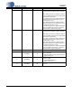
7.2 Analog Inputs
The analog inputs of the CS4207 can be configured as single-ended, pseudo-differential, or fully differential
topologies. See Tables 5 and 6 for the register settings required to place the analog inputs into the appro-
priate topology. The ADC1 Gain, ADC2 Gain, ADC1 PGA Mode, and ADC2 PGA Mode bits are located in
the ADC Configuration (CIR = 0002h) register of the Vendor Processing Widget (Node ID = 11h).
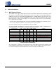
Table 5. Line In 1/Mic In 2 Input Topology Register Settings
Table 6. Mic In 1/Line In 2 Input Topology Register Settings
Note:
Alternatively, the BTL bit in the Mic In 1/Line In 2 EAPD/BTL Enable control of the Mic In 1/Line In
2 Pin Widget (Node ID = 0Dh) may be set to ‘1’b to put ADC2 in fully differential mode.
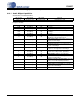
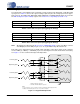
Both analog stereo input pairs may be used with single-ended line or microphone inputs. In this configura-
tion the LINEIN_C-, MICIN_L-, and MICIN_R- pins are internally disconnected and should be left floating.
See Figure 11 for the recommended single-ended input filter.
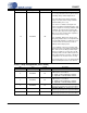
ADC1 Gain ADC1 PGA Mode Figure
Single-Ended 0 1 11
Pseudo-Differential (default) 0 0 12
ADC2 Gain (Note:) ADC2 PGA Mode Figure
Single-Ended 0 1 11
Pseudo-Differential (default) 0 0 12
Fully Differential 1 0 13
LINEIN_L+
1800 pF
1800 pF
100 k
100
LINEIN_R+
*
*
1 µF
1 µF
100 k
100
NPO/C0G dielectric capacitors.
Note:
1. These capacitors serve as a charge reservoir for the internal switched capacitor ADC
modulators and should be placed as close as possible to the inputs.
Note 1
*
Low ESR, X7R/X5R dielectric capacitors.
**
**
**
MICIN_L+
1800 pF
1800 pF
100 k
100
MICIN_R+
*
*
1 µF
1 µF
100 k
100
**
**
LINEIN_C-
MICIN_L-
MICIN_R-
N/C
N/C
CS4207
+
-
PGA
-
+
PGA
-
+
PGA
+
-
PGA
AGND
//
Left Analog Input 1
//
Right Analog Input 1
//
Left Analog Input 2
//
Right Analog Input 2
N/C
VCOM
VCOM
VCOM
Figure 11. Single-Ended Input Filter