CS4205 CrystalClear® Audio Codec ’97 for Portable Computing ! Three Features ! Integrated 2 Asynchronous I S Input Port (ZV Port) ! Integrated High-Performance Microphone Pre-Amplifier ! Integrated Digital Effects Processing for Bass and Treble Response ! Digital Docking Including an I2S Output, 3 Synchronous I2S Inputs ! Performance Oriented Digital Mixer ! SRS© 3D Stereo Enhancement ! On-chip PLL for use with External Clock Sources ! Dedicated Microphone Analog-to-Digital Converter ! Sample Rate Conve
CS4205 TABLE OF CONTENTS 1. CHARACTERISTICS AND SPECIFICATIONS ........................................................................ 6 ANALOG CHARACTERISTICS ................................................................................................ 6 ABSOLUTE MAXIMUM RATINGS ........................................................................................... 7 RECOMMENDED OPERATING CONDITIONS ....................................................................... 7 AC ’97 SERIAL PORT TIMING.
CS4205 4.2.5 GPIO Pin Status (Slot 12) ............................................................................................. 22 4.3 AC-Link Protocol Violation - Loss of SYNC ..................................................................... 23 5. REGISTER INTERFACE .................................................................................................... 24 5.1 Reset Register (Index 00h) .............................................................................................. 26 5.
CS4205 11. 12. 13. 14. 15. 16. 17. 18. 10.1.3 New Warm Reset .............................................................................................. 59 10.1.4 Register Reset .................................................................................................. 59 10.2 Powerdown Controls ...................................................................................................... 60 CLOCKING ......................................................................................
CS4205 Figure 25. Line Input (Replicate for Video and AUX) .................................................................... 64 Figure 26. Differential 2 VRMS CD Input ...................................................................................... 64 Figure 27. Differential 1 VRMS CD Input ...................................................................................... 64 Figure 28. Microphone Input .............................................................................................
CS4205 LIST OF TABLES Table 1. AC Mode Control Configurations ........................................................................16 Table 2. Register Overview for the CS4205 .....................................................................24 Table 3. Indirectly Addressed Register Overview .............................................................25 Table 4. Analog Mixer Output Attenuation ........................................................................26 Table 5. Tone Control Values ....
CS4205 1. CHARACTERISTICS AND SPECIFICATIONS ANALOG CHARACTERISTICS (Standard test conditions unless otherwise noted: Tambient = 25° C, AVdd = 5.0 V ±5%, DVdd = 3.3 V ±5%; 1 kHz Input Sine wave; Sample Frequency, Fs = 48 kHz; ZAL=100 kΩ/ 1000 pF load for Mono and Line Outputs; CDL = 18 pF load (Note 1); Measurement bandwidth is 20 Hz - 20 kHz, 18-bit linear coding for ADC functions, 20-bit linear coding for DAC functions; Mixer registers set for unity gain.
CS4205 ANALOG CHARACTERISTICS (Continued) Parameter (Note 2) Symbol External Load Impedance Line Output, Mono Output Output Impedance Line Output, Mono Output Input Capacitance Vrefout Path (Note 3) (Note 4) (Note 4) CS4205-KQZ Unit Min Typ Max 10 - - kΩ 2.3 730 5 2.4 2.
CS4205 DIGITAL CHARACTERISTICS (AVss1 = AVss2 = DVss1 = DVss2 = 0 V) Parameter DVdd = 3.3V Low level input voltage High level input voltage High level output voltage Low level output voltage Input Leakage Current (AC-link inputs) Output Leakage Current (Tri-stated AC-link outputs) Output buffer drive current BIT_CLK, SPDO/SDO2 SDATA_IN, EAPD/SCLK, GPIO0/LRCLK, GPIO1/SDOUT, GPIO2/SDI1, GPIO3/SDI2, GPIO4/SDI3 (Note 4) DVdd = 5.
CS4205 AC ’97 SERIAL PORT TIMING Standard test conditions unless otherwise noted: Tambient = 25° C, AVdd = 5.0 V, DVdd = 3.3 V; CL = 55 pF load.
CS4205 BIT_CLK Trst_low Trst2clk RESET# Tvdd2rst# Vdd Figure 1. Power Up Timing BIT_CLK SYNC Tsync2crd CODEC_READY Figure 2. Codec Ready from Start-up or Fault Condition BIT_CLK Torise Tifall Tclk_high Tclk_low Tclk_period SYNC Tirise Tsync_high Tifall Tsync_low Tsync_period Figure 3.
CS4205 BIT_CLK SDATA_IN Tco SDATA_OUT, SYNC Tisetup Tihold Figure 4. Data Setup and Hold BIT_CLK Slot 1 SDATA_OUT Write to 0x20 Slot 2 Data PR4 Don't Care Ts2_pdown SDATA_IN SYNC Tsync_pr4 Tsync2clk Figure 5. PR4 Powerdown and Warm Reset RESET# Tsetup2rst SDATA_OUT, SYNC Toff SDATA_IN, BIT_CLK Hi-Z Figure 6.
CS4205 2. GENERAL DESCRIPTION 2.1 The CS4205 is a mixed-signal serial audio codec compliant with the Intel® Audio Codec ’97 Specification, revision 2.1 [6] (referred to as AC ’97). It is designed to be paired with a digital controller, typically located on the PCI bus or integrated within the system core logic chip set. The controller is responsible for all communications between the CS4205 and the remainder of the system. The CS4205 contains two distinct functional sections: digital and analog.
CS4205 2.2 Control Registers The CS4205 contains a set of AC ’97 compliant control registers, and a set of Cirrus Logic defined control registers. These registers control the basic functions and features of the CS4205. Read accesses of the control registers by the AC ’97 controller are accomplished with the requested register index in Slot 1 of a SDATA_OUT frame. The following SDATA_IN frame will contain the read data in Slot 2.
CS4205 PC BEEP BYPASS MUTE VOL MUTE VOL MUTE VOL PHONE VOL PC_BEEP MUTE Front D/A CONVERTERS PCM_OUT MIC1 MIC2 MUTE MUTE Σ Σ MASTER VOLUME VOL MUTE VOL AUX MUTE VOL VIDEO DAC DIRECT MODE ANALOG STEREO INPUT MIXER VOL CD BOOST VOL LINE DAC MIC SELECT LINE OUT MUTE OUTPUT BUFFER MUTE OUTPUT BUFFER ANALOG STEREO OUTPUT MIXER MONO MIX SELECT STEREO TO MONO MIXER Σ MONO OUT SELECT MONO OUT VOL 1/2 STEREO TO MONO MIXER MONO VOLUME Σ 1/2 L/R ADC GAIN VOL ADC INPUT MUX
CS4205 DAC surr ch MIC MIXER mux out DACS ADC mic out mix out SRC AUX Analog centric mode is detailed in Figure 10 on page 18. In this mode, all the digital sources are pre-mixed in the digital mixer and sent to the DACs. The DAC outputs are mixed with the analog sources in the analog mixer. The ADCs send captured data directly to the host. The ADC mux is used to select a single source or the output of the input mixer for capture.
CS4205 3.2 output of the digital mixer is captured by the host. Any mixing with host sources and effects processing is done on the host. The processed signal is sent to the DACs, bypassing the analog mixer using DAC direct mode. In host processing mode, the playback and capture paths are completely separate inside the CS4205. Digital Centric Mode Digital centric mode is detailed in Figure 11. In this mode, the analog sources are first mixed in the analog mixer and sent to the ADCs.
surr ch mux out mic out ADC ½ ADC VOL VOL I²S IN2 VOL Σ DIG EFX VOL MIC AUX CD LINE ADC MICS I²S IN1 mic out LINE_OUT Σ ½ ADC c+lfe ch MONO_OUT L/R cap SRC mic cap ½ SRC AC-Link ½ SRC AC-Link mic cap MIXER mux out Σ MONO_OUT SRC DAC surr ch c+lfe ch L/R cap SRC LINE_OUT VIDEO MIC AUX MIXER mix out DAC front ch mix out SRC CD LINE front ch VIDEO CS4205 MICS I²S OUT1 VOL I²S IN1 VOL I²S IN2 VOL I²S IN3 VOL Σ SDOS VOL S/PDIF OUT VOL ZV surr ch
CS4205 within the frame. The first bit position in a new serial data frame is F0 and the last bit position in the serial data frame is F255. When SYNC goes active (high) and is sampled active by the CS4205 (on the falling edge of BIT_CLK), both devices are synchronized to a new serial data frame. The data on the SDATA_OUT pin at this clock edge is the final bit of the previous frame’s serial data. On the next rising edge of BIT_CLK, the first bit of Slot 0 is driven by the controller on the SDATA_OUT pin.
CS4205 4.1 AC-Link Serial Data Output Frame In the serial data output frame, data is passed on the SDATA_OUT pin to the CS4205 from the AC ’97 controller. Figure 14 illustrates the serial port timing. The PCM playback data being passed to the CS4205 is shifted out MSB first in the most significant bits of each slot. Any PCM data from the AC ’97 controller that is not 20 bits wide should be left justified in its corresponding slot and dithered or zero-padded in the unused bit positions.
CS4205 4.1.3 Command Data Port (Slot 2) Bit 19 18 17 16 15 14 13 12 11 10 9 8 7 6 5 4 WD15 WD14 WD13 WD12 WD11 WD10 WD9 WD8 WD7 WD6 WD5 WD4 WD3 WD2 WD1 WD0 3 2 1 0 Reserved WD[15:0] Write Data. The WD[15:0] bits contain the 16-bit value to be written to the register. If an access is a read, this slot is ignored. NOTE: For any write to an AC ’97 register, the write is defined to be an ‘atomic’ access.
CS4205 4.2 AC-Link Serial Data Input Frame In the serial data input frame, data is passed on the SDATA_IN pin from the CS4205 to the AC ’97 controller. The data format for the input frame is very similar to the output frame. Figure 14 on page 19 illustrates the serial port timing. The PCM capture data from the CS4205 is shifted out MSB first in the most significant 18 bits of each slot. The least significant 2 bits in each slot will be ‘cleared’.
CS4205 4.2.3 Status Data Port (Slot 2) Bit 19 18 17 16 15 14 13 12 11 10 9 8 7 6 5 4 RD15 RD14 RD13 RD12 RD11 RD10 RD9 RD8 RD7 RD6 RD5 RD4 RD3 RD2 RD1 RD0 RD[15:0] 4.2.4 3 2 1 0 Reserved Read Data. The RD[15:0] bits contain the register data requested by the controller from the previous read request. All read requests will return the read address in the input Slot 1 and the register data in the input Slot 2 on the following serial data frame.
CS4205 4.3 AC-Link Protocol Violation - Loss of SYNC The CS4205 is designed to handle SYNC protocol violations. The following are situations where the SYNC protocol has been violated: • The SYNC signal is not sampled high for exactly 16 BIT_CLK clock cycles at the start of an audio frame. • The SYNC signal is not sampled high on the 256th BIT_CLK clock period after the previous SYNC assertion.
CS4205 5.
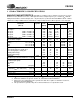
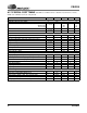
CS4205 Reg Register Name D15 D14 D13 D12 D11 D10 D9 D8 D7 D6 00h PCM Input Volume Mute 0 GL5 GL4 GL3 GL2 GL1 GL0 0 0 GR5 GR4 GR3 GR2 GR1 GR0 8000h 01h ADC Input Volume Mute 0 GL5 GL4 GL3 GL2 GL1 GL0 0 0 GR5 GR4 GR3 GR2 GR1 GR0 8000h 02h SDI1 Volume Mute 0 GL5 GL4 GL3 GL2 GL1 GL0 0 0 GR5 GR4 GR3 GR2 GR1 GR0 8000h 03h SDI2 Volume Mute 0 GL5 GL4 GL3 GL2 GL1 GL0 0 0 GR5 GR4 GR3 GR2 GR1 GR0 8000h 04h SDI3 Volume Mute 0 GL5 GL4 GL3 GL2 GL1
CS4205 5.1 D15 0 Reset Register (Index 00h) D14 SE4 D13 SE3 D12 SE2 D11 SE1 D10 SE0 D9 0 D8 ID8 D7 ID7 D6 0 D5 ID5 D4 0 D3 ID3 D2 ID2 D1 0 SE[4:0] SRS 3D Stereo Enhancement. SE[4:0] = 01001, indicating this feature is present. ID8 18-bit ADC Resolution. The ID8 bit is ‘set’, indicating this feature is present. ID7 20-bit DAC resolution. The ID7 bit is ‘set’, indicating this feature is present. ID5 Loudness. The ID5 bit is ‘set’, indicating this feature is present.
CS4205 5.3 Mono Volume Register (Index 06h) D15 Mute D14 0 D13 0 D12 0 D11 0 D10 0 D9 0 D8 0 D7 0 D6 0 D5 MM5 D4 MM4 D3 MM3 D2 MM2 D1 MM1 D0 MM0 Mute Mono Mute. Setting this bit mutes the MONO_OUT output signal. MM[5:0] Mono Volume Control. The MM[5:0] bits control the mono output volume. Each step corresponds to 1.5 dB gain adjustment, with a total available range from 0 dB to -46.5 dB attenuation. Setting the MM5 bit sets the mono attenuation to -46.
CS4205 5.5 D15 Mute PC_BEEP Volume Register (Index 0Ah) D14 0 D13 0 D12 0 D11 0 D10 0 D9 0 D8 0 D7 0 D6 0 D5 0 D4 PV3 D3 PV2 D2 PV1 D1 PV0 D0 0 Mute PC_BEEP Mute. Setting this bit mutes the PC_BEEP input signal. PV[3:0] PC_BEEP Volume Control. The PV[3:0] bits control the gain levels of the PC_BEEP input source to the Input Mixer. Each step corresponds to 3 dB gain adjustment, with 0000 = 0 dB. The total range is 0 dB to -45 dB attenuation. Default 0000h.
CS4205 5.7 D15 Mute Microphone Volume Register (Index 0Eh) D14 0 D13 0 D12 0 D11 0 D10 0 D9 0 D8 0 D7 0 D6 20dB D5 0 D4 GN4 D3 GN3 D2 GN2 D1 GN1 D0 GN0 Mute Microphone Mute. Setting this bit mutes the MIC1 or MIC2 signal. The selection of the MIC1 or MIC2 input pin is controlled by the MS bit in the General Purpose Register (Index 20h). 20dB Microphone 20 dB Boost. When ‘set’, the 20dB bit enables the +20 dB microphone boost block. In combination with the 10dB boost bit in the Misc.
CS4205 5.8 D15 Mute Analog Mixer Input Gain Registers (Index 10h - 18h) D14 0 D13 0 D12 GL4 D11 GL3 D10 GL2 D9 GL1 D8 GL0 D7 0 D6 0 D5 0 D4 GR4 D3 GR3 D2 GR2 D1 GR1 D0 GR0 Mute Stereo Input Mute. Setting this bit mutes the respective input signal, both right and left inputs. GL[4:0] Left Volume Control. The GL[4:0] bits are used to control the gain level of the left analog input source to the Input Mixer. Each step corresponds to 1.5 dB gain adjustment, with 01000 = 0 dB.
CS4205 5.9 D15 0 Input Mux Select Register (Index 1Ah) D14 0 D13 0 D12 0 D11 0 D10 SL2 D9 SL1 D8 SL0 D7 0 D6 0 D5 0 D4 0 D3 0 D2 SR2 D1 SR1 D0 SR0 SL[2:0] Left Channel Source. The SL[2:0] bits select the left channel source to pass to the ADCs for recording. See Table 9 for possible values. SR[2:0] Right Channel Source. The SR[2:0] bits select the right channel source to pass to the ADCs for recording. See Table 9 for possible values. Default 0000h.
CS4205 5.10 D15 Mute Record Gain Register (Index 1Ch) D14 0 D13 0 D12 0 D11 GL3 D10 GL2 D9 GL1 D8 GL0 D7 0 D6 0 D5 0 D4 0 D3 GR3 D2 GR2 D1 GR1 D0 GR0 Mute Record Gain Mute. Setting this bit mutes the input to the L/R ADCs. GL[3:0] Left ADC Gain. The GL[3:0] bits control the input gain on the left channel of the analog source, applied after the input mux and before the ADCs. Each step corresponds to 1.5 dB gain adjustment, with 0000 = 0 dB. The total range is 0 dB to +22.5 dB gain.
CS4205 5.12 D15 POP General Purpose Register (Index 20h) D14 ST D13 3D D12 LD D11 0 D10 0 D9 MIX D8 MS D7 LPBK D6 0 D5 0 D4 0 D3 0 D2 0 D1 0 D0 0 POP PCM Out Path. When ‘clear’, the PCM out path is mixed pre 3D. When ‘set’, the PCM out path is mixed post 3D. ST Stereo Enhancement Enable. When ‘set’, the ST bit enables the simulated stereo enhancement via the SRS Mono algorithm. 3D 3D Enable. When ‘set’, the 3D bit enables the 3D stereo enhancement via the SRS Stereo algorithm.
CS4205 5.14 D15 EAPD Powerdown Control/Status Register (Index 26h) D14 0 D13 PR5 D12 PR4 D11 PR3 D10 PR2 D9 PR1 D8 PR0 D7 0 D6 0 D5 0 D4 0 D3 REF D2 ANL D1 DAC D0 ADC EAPD External Amplifier Power Down. The EAPD pin follows this bit and is generally used to power down external amplifiers. The EAPD bit is mutually exclusive with the SDSC bit in the Serial Port Control Register (Index 6Ah). The SDSC bit must be ‘clear’ before the EAPD bit may be ‘set’.
CS4205 5.15 D15 ID1 Extended Audio ID Register (Index 28h) D14 ID0 D13 0 D12 0 D11 0 D10 0 D9 AMAP D8 0 D7 0 D6 0 D5 0 D4 0 D3 VRM D2 0 D1 0 D0 VRA ID[1:0] Codec ID. These bits indicate the current codec configuration. When ID[1:0] = 00, the CS4205 is the primary audio codec. When ID[1:0] = 01, 10, or 11, the CS4205 is a secondary audio codec. The state of the ID[1:0] bits is determined at power-up from the ID[1:0]# pins and the current clocking scheme, see Table 27 on page 63.
CS4205 5.16 D15 0 Extended Audio Status/Control Register (Index 2Ah) D14 PRL D13 0 D12 0 D11 0 D10 0 D9 MADC D8 0 D7 0 D6 0 D5 0 D4 0 D3 VRM D2 0 D1 0 D0 VRA PRL Mic ADC Powerdown. When ‘set’, the PRL bit powers down the dedicated Mic ADC and corresponding input gain stage. To use the dedicated Mic ADC, clear the PRL bit first. MADC Mic ADC Ready Status. When ‘set’, the MADC bit indicates the dedicated Mic ADC is ready to transmit data. VRM Enable Variable Rate Mic Audio.
CS4205 5.17 D15 SR15 Audio Sample Rate Control Registers (Index 2Ch - 34h) D14 SR14 D13 SR13 D12 SR12 D11 SR11 D10 SR10 D9 SR9 D8 SR8 D7 SR7 D6 SR6 D5 SR5 D4 SR4 D3 SR3 D2 SR2 D1 SR1 D0 SR0 SR[15:0] Sample Rate Select. The Audio Sample Rate Control Registers (Index 2Ch - 34h) control playback and capture sample rates. The PCM Front DAC Rate Register (Index 2Ch) controls the Front Left and Front Right DAC sample rates.
CS4205 5.18 D15 ID1 Extended Modem ID Register (Index 3Ch) D14 ID0 D13 0 D12 0 D11 0 D10 0 D9 0 D8 0 D7 0 D6 0 D5 0 D4 0 D3 0 D2 0 D1 0 D0 0 ID[1:0] Codec ID. These bits indicate the current codec configuration. When ID[1:0] = 00, the CS4205 is the primary audio codec. When ID[1:0] = 01, 10, or 11, the CS4205 is a secondary audio codec. The state of the ID[1:0] bits is determined at power-up from the ID[1:0]# pins and the current clocking scheme, see Table 27 on page 63. Default x000h.
CS4205 5.21 D15 1 GPIO Pin Polarity/Type Configuration Register (Index 4Eh) D14 1 D13 1 D12 1 D11 1 D10 1 D9 1 D8 1 D7 1 D6 1 D5 1 D4 GP4 D3 GP3 D2 GP2 D1 GP1 D0 GP0 GP[4:0] GPIO Pin Configuration. This register defines the GPIO input polarity (0 = Active Low, 1 = Active High) when a GPIO pin is configured as an input. The GP[4:0] bits define the GPIO output type (0 = CMOS, 1 = OPEN-DRAIN) when a GPIO pin is configured as an output.
CS4205 5.23 GPIO Pin Wakeup Mask Register (Index 52h) D15 0 D14 0 D13 0 D12 0 D11 0 D10 0 D9 0 D8 0 D7 0 D6 0 D5 0 D4 GW4 D3 GW3 D2 GW2 D1 GW1 D0 GW0 GW[4:0] GPIO Pin Wakeup. This register provides a mask for determining if an input GPIO change will generate a wakeup event (0 = no, 1 = yes). When the AC-link is powered up, a wakeup event will be communicated through the assertion of GPIO_INT = 1 in input Slot 12.
CS4205 CAPS[1:0] L/R Capture Source Select. The CAPS[1:0] bits control the source of data routed to the L/R ADC slots, see Table 14 for actual slots used. Table 15 lists the available capture options. If a reserved source is selected, the capture slot data will be fixed to ‘0’. MICS Microphone Capture Source Select. The MICS bit selects the source of data routed to the Mic ADC slot. If this bit is ‘clear’, the Mic capture slot will receive data from the Mic ADC.
CS4205 Codec ID Slot Assignment Mode Slot Map Slot Assignments DAC ID1 ID0 SM1 SM0 AMAP SDO2 SPDIF for SPDS = 00 SDOUT ADC SPDIF for SPDS = 01 L R L R L R L R M AMAP Mode 0 0 0 X X 1 3 4 7 8 6 9 3 4 6 AMAP Mode 1 0 1 X X 1 3 4 7 8 6 9 3 4 6 AMAP Mode 2 1 0 X X 1 7 8 6 9 10 11 7 8 6 AMAP Mode 3 1 1 X X 1 6 9 7 8 10 11 7 8 6 Slot Map Mode 0 X X 0 0 0 3 4 7 8 6 9 3 4 6 Slot Map Mode 1 X X 0 1 0 7 8 6 9 10 1
CS4205 5.26 D15 0 Misc. Crystal Control Register (Index 60h) D14 0 D13 Res D12 DPC D11 0 D10 0 D9 D8 Reserved D7 D6 10dB CRST D5 D4 Reserved D3 GPOC D2 D1 Reserved D0 LOSM DPC DAC Phase Control. This bit controls the phase of the PCM stream sent to the DACs (after SRC). When ‘cleared’ the phase of the signal will remain unchanged. When this bit is ‘set’, each PCM sample will be inverted before being sent to the DACs. 10dB Microphone 10 dB Boost.
CS4205 5.27 D15 SPEN S/PDIF Control Register (Index 68h) D14 Val D13 0 D12 Fs D11 L D10 CC6 D9 CC5 D8 CC4 D7 CC3 D6 CC2 D5 CC1 D4 CC0 D3 Emph D2 D1 Copy /Audio D0 Pro SPEN S/PDIF Enable. The SPEN bit enables S/PDIF data transmission on the SPDO/SDO2 pin. The SPEN bit routes the left and right channel data from the AC ’97 controller, the digital mixer, or the digital effects engine to the S/PDIF transmitter block.
CS4205 5.28 Serial Port Control Register (Index 6Ah) D15 SDEN D14 0 D13 0 D12 0 D11 0 D10 0 D9 0 D8 0 D7 0 D6 SDI3 D5 SDI2 D4 SDI1 D3 D2 D1 D0 SDO2 SDSC SDF1 SDF0 SDEN Serial Data Output Enable. The SDEN bit enables transmission of serial data on the SDOUT pin. The SDEN bit routes the left and right channel data from the AC ’97 controller, the digital mixer, or the digital effects engine to the serial data port.
CS4205 5.29 Special Feature Address Register (Index 6Ch) D15 0 D14 0 D13 0 D12 0 D11 0 D10 0 D9 0 D8 0 D7 0 D6 0 D5 0 D4 0 D3 A3 D2 A2 D1 A1 D0 A0 A[3:0] Special Feature Address. This register functions as an index register to select the desired functionality of the Special Feature Data Register (Index 6Eh). Before using any of these indexed registers, the correct index value must be written to bits A[3:0]. Default 0000h 5.
CS4205 5.32 D15 Mute Serial Data Port Volume Control Registers (Index 6Eh, Address 06h - 07h) D14 0 D13 GL5 D12 GL4 D11 GL3 D10 GL2 D9 GL1 D8 GL0 D7 0 D6 0 D5 GR5 D4 GR4 D3 GR3 D2 GR2 D1 GR1 D0 GR0 Mute Serial Data Port Mute. Setting this bit mutes the respective input signal, both left and right inputs. GL[5:0] Left Volume Control. The GL[5:0] bits are used to control the serial data port left channel output volume. Each step corresponds to 1 dB gain adjustment.
CS4205 5.33 D15 Res Signal Processing Engine Control Register (Index 6Eh, Address 08h) D14 D13 D12 D11 D10 D9 D8 D7 SDI1M SRZC1 SRZC0 LPFS1 LPFS0 HPFS1 HPFS0 GL3 D6 GL2 D5 GL1 D4 GL0 D3 GR3 D2 GR2 D1 GR1 D0 GR0 SDI1M Serial Data Input 1 Mode. The SDI1M bit controls the flow of data from the first serial data input into the signal processing engine. If this bit is ‘0’, the two channels of the SDI1 port are routed to their respective channels of the SDI1 volume control.
CS4205 5.
CS4205 5.35 BIOS-Driver Interface Control Registers (Index 6Eh, Address 0Ch - 0Dh) D15 E15 D14 E14 D13 E13 D12 E12 D11 E11 D10 E10 D9 E9 D8 E8 D7 E7 D6 E6 D5 E5 D4 E4 D3 E3 D2 E2 D1 E1 E[15:0] Event Configuration. The E[15:0] bits control the BIOS-Driver Interface mechanism. Default 0000h D0 E0 The BDI Config Register (Index 6Eh, Address 0Ch) enables BIOS-Driver communication for each possible event. If a bit is ‘0’, the corresponding event will not be communicated.
CS4205 Default 0000h The BDI Status Register (Index 7Ah) reflects the state of all possible events. If a bit is ‘0’, the corresponding event has not occurred or has already been handled by the driver. If a bit is ‘1’, the corresponding event has occurred and has not been handled by the driver yet. The BDI bit in input slot 12 is a logic OR of all bits in this register ANDed with their corresponding bit in the BDI Config Register (Index 6Eh, Address 0Ch).
CS4205 5.38 Vendor ID1 Register (Index 7Ch) D15 F7 D14 F6 D13 F5 D12 F4 D11 F3 D10 F2 D9 F1 D8 F0 D7 S7 D6 S6 D5 S5 D4 S4 D3 S3 D2 S2 D1 S1 D0 S0 F[7:0] First Character of Vendor ID. With a value of F[7:0] = 43h, these bits define the ASCII ‘C’ character. S[7:0] Second Character of Vendor ID. With a value of S[7:0] = 52h, these bits define the ASCII ‘R’ character. Default 4352h. This register contains read-only data. 5.
CS4205 versed. This DAC phase reversal is controlled by the DPC bit in the Misc. Crystal Control Register (Index 60h). This feature is necessary since the phase response for external DACs is unknown and the phase response of the internal DACs can vary depending on the path determined by the DDM bit in the AC Mode Control Register (Index 5Eh). This feature guarantees that all DACs in a system have the same phase response, maintaining the accuracy of spatial cues. 6. SERIAL DATA PORTS 6.
CS4205 6.3 Digital Docking The CS4205 features three serial data input ports used to receive data from three stereo ADCs inside a docking station. One serial data output port is used to transmit data to a stereo DAC inside the docking station. To fully utilize digital docking, the CS4205 should be configured for digital centric mode; see Section 3.2, Digital Centric Mode. This will allow the docking sources to be mixed with the analog sources from the notebook.
CS4205 SDF[1:0] 00 01 10 11 LRCLK Data Data Alignment Data Timing Polarity Justification (MSB vs. LRCLK) Resolution Diagram Recommended DAC/ADC negative positive positive positive CS4334/CS5331A CS4335/CS5330A CS4337/none CS4338/none left justified left justified right justified right justified 1 SCLK delayed not delayed not delayed not delayed 20-bit 20-bit 20-bit 16-bit Figure 17 Figure 18 Figure 19 Figure 20 Table 23.
CS4205 7. ZV PORT The CS4205 implements an asynchronous serial data input port that conforms to the Zoomed Video Port (ZV Port) specification. ZV Port data is asynchronous I2S data in PCM format with 16 bits of resolution. The ZV Port interface consists of four signals: MCLK, SCLK, LRCLK, and SDATA. However, the CS4205 does not require a connection to the asynchronous MCLK. The other three signals are respectively received on ZSCLK, ZLRCLK, and ZSDATA.
CS4205 8. SONY/PHILIPS DIGITAL INTERFACE (S/PDIF) The S/PDIF digital output is used to interface the CS4205 to consumer audio equipment external to the PC. This output provides an interface for storing digital audio data or playing digital audio data to digital speakers. Figure 22 illustrates the circuits necessary for implementing the IEC-958 optical or consumer interface. For further information on S/PDIF operation see application note AN22: Overview of Digital Audio Interface Data Structures [3].
CS4205 10. POWER MANAGEMENT 10.1 AC ’97 Reset Modes The CS4205 supports four reset methods, as defined in the AC ’97 Specification: Cold Reset, Warm Reset, New Warm Reset, and Register Reset. A Cold Reset results in all AC ’97 logic (registers included) initialized to its default state. A Warm Reset or New Warm Reset leaves the contents of the AC ’97 register set unaltered. A Register Reset initializes only the AC ’97 registers to their default states. 10.1.
CS4205 10.2 Powerdown Controls The Powerdown Control/Status Register (Index 26h) controls the power management functions. The PR[5:0] bits in this register control the internal powerdown states of the CS4205. Powerdown control is available for individual subsections of the CS4205 by asserting any PRx bit or any combination of PRx bits. All powerdown states except PR4 and PR5 can be resumed by clearing the corresponding PRx bit.
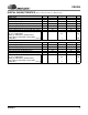
CS4205 PR Bit ADCs PR0 • DACs Mixer • • • • • PR1 PR2 PR3 • • Analog Reference Internal Clock Off Mic ADC • • • • PR4 PR5 AC Link • • • • • PRL Table 25. Powerdown PR Function Matrix for the CS4205 IDVdd1 (mA) [DVdd=3.
CS4205 11. CLOCKING 11.2 The CS4205 may be operated as a primary or secondary codec. As a primary codec, the system clock for the AC-link may be generated from an external 24.576 MHz clock source, a 24.576 MHz crystal, or the internal Phase Locked Loop (PLL). The PLL allows the CS4205 to accept external clock frequencies other than 24.576 MHz. As a secondary codec, the system clock is derived from BIT_CLK, which is generated by the primary codec.
CS4205 XTL_IN XTL_OUT 24.576 MHz 22 pF 22 pF DGND Figure 24. External Crystal External Clock on ID1# ID0# XTL_IN Yes Yes Yes Yes No No No No 1 1 0 0 1 1 0 0 1 0 1 0 1 0 1 0 AC-Link Timing Mode Codec ID Clock Source Clock Rate (MHz) PLL Active Primary Primary Primary Primary Primary Secondary Secondary Secondary 0 0 0 0 0 1 2 3 External External External External XTAL BIT_CLK BIT_CLK BIT_CLK 24.576 14.31818 27.000 48.000 24.576 12.288 12.288 12.
CS4205 12. ANALOG HARDWARE DESCRIPTION The analog input section consists of four stereo line-level inputs (LINE_L/R, CD_L/GND/R, VIDEO_L/R, and AUX_L/R), two selectable mono microphone inputs (MIC1 and MIC2), and two mono inputs (PC_BEEP and PHONE). The analog output section consists of a mono output (MONO_OUT) and a stereo line-level output (LINE_OUT_L/R). This section describes the analog hardware needed to interface with these pins.
CS4205 12.1.3 Microphone Inputs 12.1.5 Phone Input Figure 28 illustrates an input circuit suitable for dynamic and electret microphones. Electret, also known as phantom-powered, microphones use the right channel (ring) of the jack for power. The design also supports the recommended advanced frequency response for voice recognition as specified in PC 99 and PC 2001. The microphone input of the CS4205 has an integrated pre-amplifier. Using combinations of the 10dB bit in the Misc.
CS4205 ence, nominally 2.4 V. This requires the outputs be AC-coupled to external circuitry (AC loads must be greater than 10 kΩ for the line output). 12.2.1 Stereo Output See Figure 31 for a stereo line-level output reference design. 12.2.2 Mono Output The mono output, MONO_OUT, can be either a sum of the left and right output channels, attenuated by 6 dB to prevent clipping at full scale, or the selected Mic signal.
CS4205 12.5 Reference Design See Section 16 for a CS4205 reference design.
CS4205 13. GROUNDING AND LAYOUT Figure 33 on page 69 shows the conceptual layout for the CS4205 in XTAL or OSC clocking modes. The decoupling capacitors should be located physically as close to the pins as possible. Also, note the connection of the REFFLT decoupling capacitors to the ground return trace connected directly to the ground return pin, AVss1. It is strongly recommended that separate analog and digital ground planes be used.
CS4205 Vrefout 1000 pF to via NPO Via to +5VA 2.2µF 0.1 µF Y5V Via to +5VA AFLT3 AFLT2 AFLT1 AVss1 REFFLT 0.1 µF Y5V AVdd1 Via to Analog Ground AVdd2 Analog Ground Via to Analog Ground AVss2 Digital Ground Via to Digital Ground Pin 1 DVdd1 0.1 µF Y5V DVss1 DVss2 0.1 µF Y5V DVdd2 Via to +5VD or +3.3VD Via to +5VD or +3.3VD Figure 33.
CS4205 SPDO/SDO2 EAPD/SCLK ID1# ID0# GPIO1/SDOUT GPIO0/LRCLK AVss2 GPIO4/SDI3 GPIO3/SDI2 GPIO2/SDI1 AVdd2 MONO_OUT 14.
CS4205 Audio I/O Pins PC_BEEP - Analog Mono Source, Input, Pin 12 The PC_BEEP input is intended to allow the PC system POST (Power On Self-Test) tones to pass through to the audio subsystem. The PC_BEEP input has two connections: the first connection is to the analog output mixer, the second connection is directly to the LINE_OUT stereo outputs. While the RESET# pin is actively being asserted to the CS4205, the PC_BEEP bypass path to the LINE_OUT outputs is enabled.
CS4205 VIDEO_L, VIDEO_R - Analog Video Audio Source, Inputs, Pins 16 and 17 These inputs form a stereo input pair to the CS4205. It is intended to be used for the audio signal output of a video device. The maximum allowable input is 1 VRMS (sinusoidal). These inputs are internally biased at the Vrefout voltage reference and require AC-coupling to external circuitry. If these inputs are not used, they should both be connected to the Vrefout pin or AC-coupled to analog ground.
CS4205 AFLT1 - Left ADC Channel Antialiasing Filter, Input, Pin 29 This pin needs a 1000 pF NPO capacitor connected to analog ground. AFLT2 - Right ADC Channel Antialiasing Filter, Input, Pin 30 This pin needs a 1000 pF NPO capacitor connected to analog ground. AFLT3 - Mic ADC Channel Antialiasing Filter, Input, Pin 31 This pin needs a 1000 pF NPO capacitor connected to analog ground.
CS4205 Clock and Configuration Pins XTL_IN - Crystal Input / Clock Input, Pin 2 This pin requires either a 24.576 MHz crystal, with the other pin attached to XTL_OUT, or an external CMOS clock. XTL_IN must have a crystal or clock source attached for proper operation except when operating in secondary codec mode. The crystal frequency must be 24.576 MHz and designed for fundamental mode, parallel resonance operation.
CS4205 This pin is a general purpose I/O pin that can be used to interface with various external circuitry. When configured as an input, it functions as a Schmitt triggered input with 350 mV hysteresis at 5 V and 220 mV hysteresis at 3.3 V. When configured as an output, it can function as a normal CMOS output (4 mA drive) or as an open drain output. This pin also provides the serial data for the first serial data port when the SDEN bit in the Serial Port Control Register (Index 6Ah) is ‘set’.
CS4205 These pins provide the supply voltage and ground for the clocking section of the CS4205. In XTAL or OSC clocking modes DVdd1 should be tied to +5 VD or to +3.3 VD, with DVss1 tied to DGND. In PLL clocking mode, DVdd1 must be tied to +5 VA and DVss1 must be tied to AGND. If connecting these pins to +5 VD or to +3.3 VD and DGND, the CS4205 and controller AC-link should share a common digital supply.
CS4205 15. PARAMETER AND TERM DEFINITIONS AC ’97 Specification Refers to the Audio Codec ’97 Component Specification Ver 2.1 published by the Intel® Corporation [6]. AC ’97 Controller or Controller Refers to the control chip which interfaces to the audio codec AC-link. This has been also called DC ’97 for Digital Controller ’97 [6]. AC ’97 Registers or Codec Registers Refers to the 64-field register map defined in the AC ’97 Specification. ADC Refers to a single Analog-to-Digital converter in the CS4205.
CS4205 Interchannel Isolation The amount of 1 kHz signal present on the output of the grounded AC-coupled line input channel with 1 kHz, 0 dB, signal present on the other line input channel. Units are in dB. Line-level Refers to a consumer equipment compatible, voltage driven interface. The term implies a low driver impedance and a minimum 10 kΩ load impedance. PATHS A-D: Analog in, through the ADCs, onto the serial link. D-A: Serial interface inputs through the DACs to the analog output.
4 3 5 2 1 AGND AGND AGND + C30 10uF ELEC 100 1.5k AGND +5VA C29 0.1uF X7R C28 + R20 R21 0.1uF X7R C22 0.1uF X7R AGND C24 1000pF NPO C25 1000pF NPO DGND C32 22pF NPO 24.576 MHz (50 PPM) Y1 2 + DGND C33 22pF NPO SPDO/SDO2 GPIO0/LRCLK GPIO1/SDOUT GPIO2/SDI1 GPIO3/SDI2 GPIO4/SDI3 ID0# ID1# EAPD/SCLK LINE_OUT_L LINE_OUT_R MONO_OUT ZLRCLK ZSDATA ZSCLK BIT_CLK SDATA_OUT SDATA_IN SYNC RESET# C6 10uF ELEC +5VA Figure 35.
CS4205 17. REFERENCES 1) Cirrus Logic, Audio Quality Measurement Specification, Version 1.0, 1997 http://www.cirrus.com/products/papers/meas/meas.html 2) Cirrus Logic, AN18: Layout and Design Rules for Data Converters and Other Mixed Signal Devices, Version 6.0, February 1998 3) Cirrus Logic, AN22: Overview of Digital Audio Interface Data Structures, Version 2.
CS4205 18. PACKAGE DIMENSIONS 48L LQFP PACKAGE DRAWING E E1 D D1 1 e B ∝ A A1 L DIM A A1 B D D1 E E1 e* L MIN --0.002 0.007 0.343 0.272 0.343 0.272 0.016 0.018 0.000° ∝ * Nominal pin pitch is 0.50 mm INCHES NOM 0.055 0.004 0.009 0.354 0.28 0.354 0.28 0.020 0.24 4° MAX 0.063 0.006 0.011 0.366 0.280 0.366 0.280 0.024 0.030 7.000° MIN --0.05 0.17 8.70 6.90 8.70 6.90 0.40 0.45 0.00° MILLIMETERS NOM 1.40 0.10 0.22 9.0 BSC 7.0 BSC 9.0 BSC 7.0 BSC 0.50 BSC 0.60 4° MAX 1.60 0.15 0.27 9.30 7.10 9.30 7.