CS4202 Audio Codec ’97 with Headphone Amplifier ! Sample Features ! AC ’97 2.
CS4202 TABLE OF CONTENTS 1. CHARACTERISTICS AND SPECIFICATIONS ........................................................................ 7 ANALOG CHARACTERISTICS ................................................................................................ 7 ABSOLUTE MAXIMUM RATINGS ........................................................................................... 8 RECOMMENDED OPERATING CONDITIONS ....................................................................... 8 AC ’97 SERIAL PORT TIMING.
CS4202 4.4 PC_BEEP Volume Register (Index 0Ah) .......................................................................... 24 4.5 Phone Volume Register (Index 0Ch) ................................................................................ 24 4.6 Microphone Volume Register (Index 0Eh)........................................................................ 25 4.7 Analog Mixer Input Gain Registers (Index 10h - 18h) ...................................................... 26 4.
CS4202 10.4 Power Supplies .............................................................................................................. 53 10.5 Reference Design .......................................................................................................... 53 11. GROUNDING AND LAYOUT .............................................................................................. 54 12. PIN DESCRIPTIONS ..............................................................................................
CS4202 LIST OF TABLES Table 1. Register Overview for the CS4202 ..................................................................... 22 Table 2. Analog Mixer Output Attenuation........................................................................ 23 Table 3. Microphone Input Gain Values ........................................................................... 25 Table 4. Analog Mixer Input Gain Values ......................................................................... 26 Table 5.
CS4202 1. CHARACTERISTICS AND SPECIFICATIONS ANALOG CHARACTERISTICS (Standard test conditions unless otherwise noted: Tambient = 25° C, AVdd = 5.0 V ±5%, DVdd = 3.3 V ±5%; 1 kHz Input Sine wave; Sample Frequency, Fs = 48 kHz; ZAL=100 kΩ/ 1000 pF load for Mono and Line Outputs; CDL = 18 pF load (Note 1); Measurement bandwidth is 20 Hz - 20 kHz, 18-bit linear coding for ADC functions, 20-bit linear coding for DAC functions; Mixer registers set for unity gain.
CS4202 ANALOG CHARACTERISTICS (Continued) Parameter (Note 2) Symbol External Load Impedance Line Output, Mono Output Headphone Output Output Impedance Line Output, Mono Output Headphone Output Input Capacitance Vrefout Path (Note 3) (Note 4) (Note 4) CS4202-JQZ Unit Min Typ Max 10 32 - - kΩ Ω 2.3 730 0.8 5 2.4 2.
CS4202 DIGITAL CHARACTERISTICS (AVss1 = AVss2 = DVss1 = DVss2 = 0 V) Parameter DVdd = 3.3V Low level input voltage High level input voltage High level output voltage Low level output voltage Input Leakage Current (AC-link inputs) Output Leakage Current (Tri-stated AC-link outputs) Output buffer drive current BIT_CLK, SDATA_IN SPDIF_OUT EAPD/SCLK, GPIO0/LRCLK, GPIO1/SDOUT, GPIO2, GPIO3, GPIO4/SDO2 (Note 4) DVdd = 5.
CS4202 AC ’97 SERIAL PORT TIMING Standard test conditions unless otherwise noted: Tambient = 25° C, AVdd = 5.0 V, DVdd = 3.3 V; CL = 55 pF load.
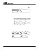
CS4202 BIT_CLK Trst_low Trst2clk RESET# Tvdd2rst# Vdd Figure 1. Power Up Timing BIT_CLK SYNC Tsync2crd CODEC_READY Figure 2. Codec Ready from Start-up or Fault Condition BIT_CLK Torise Tifall Tclk_high Tclk_low Tclk_period SYNC Tirise Tsync_high Tifall Tsync_low Tsync_period Figure 3.
CS4202 BIT_CLK SDATA_IN Tco SDATA_OUT, SYNC Tisetup Tihold Figure 4. Data Setup and Hold BIT_CLK Slot 1 SDATA_OUT Write to 0x20 Slot 2 Data PR4 Don't Care Ts2_pdown SDATA_IN SYNC Tsync_pr4 Tsync2clk Figure 5. PR4 Powerdown and Warm Reset RESET# Tsetup2rst SDATA_OUT, SYNC Toff SDATA_IN, BIT_CLK Hi-Z Figure 6.
CS4202 2. GENERAL DESCRIPTION 2.1 The CS4202 is a mixed-signal serial audio codec with integrated headphone power amplifier compliant with the Intel® Audio Codec ’97 Specification, revision 2.2 [6] (referred to as AC ’97). It is designed to be paired with a digital controller, typically located on the PCI bus or integrated within the system core logic chip set. The controller is responsible for all communications between the CS4202 and the remainder of the system.
CS4202 2.2 Control Registers The CS4202 contains a set of AC ’97 compliant control registers, and a set of Cirrus Logic defined control registers. These registers control the basic functions and features of the CS4202. Read accesses of the control registers by the AC ’97 controller are accomplished with the requested register index in Slot 1 of a SDATA_OUT frame. The following SDATA_IN frame will contain the read data in Slot 2.
CS4202 PC BEEP BYPASS MUTE VOL MUTE VOL MUTE VOL PHONE VOL PC_BEEP MUTE MAIN D/A CONVERTERS PCM_OUT MIC1 MIC2 DAC DIRECT MODE ANALOG STEREO INPUT MIXER MUTE Σ Σ MASTER VOLUME VOL MUTE VOL CD BOOST VOL LINE DAC MIC SELECT ANALOG STEREO OUTPUT MIXER LINE OUT MUTE OUTPUT BUFFER MUTE HEADPHONE AMPLIFIER MUTE OUTPUT BUFFER HEADPHONE VOLUME HEADPHONE OUT VOL MUTE VOL AUX VOL VIDEO MUTE MONO MIX SELECT STEREO TO MONO MIXER Σ MONO OUT SELECT MONO OUT VOL 1/2 STEREO TO M
CS4202 within the frame. The first bit position in a new serial data frame is F0 and the last bit position in the serial data frame is F255. When SYNC goes active (high) and is sampled active by the CS4202 (on the falling edge of BIT_CLK), both devices are synchronized to a new serial data frame. The data on the SDATA_OUT pin at this clock edge is the final bit of the previous frame’s serial data. On the next rising edge of BIT_CLK, the first bit of Slot 0 is driven by the controller on the SDATA_OUT pin.
CS4202 3.1 AC-Link Serial Data Output Frame In the serial data output frame, data is passed on the SDATA_OUT pin to the CS4202 from the AC ’97 controller. Figure 9 illustrates the serial port timing. The PCM playback data being passed to the CS4202 is shifted out MSB first in the most significant bits of each slot. Any PCM data from the AC ’97 controller that is not 20 bits wide should be left justified in its corresponding slot and dithered or zero-padded in the unused bit positions.
CS4202 3.1.3 Command Data Port (Slot 2) Bit 19 18 17 16 15 14 13 12 11 10 9 8 7 6 5 4 WD15 WD14 WD13 WD12 WD11 WD10 WD9 WD8 WD7 WD6 WD5 WD4 WD3 WD2 WD1 WD0 3 2 1 0 Reserved WD[15:0] Write Data. The WD[15:0] bits contain the 16-bit value to be written to the register. If an access is a read, this slot is ignored. NOTE: For any write to an AC ’97 register, the write is defined to be an ‘atomic’ access.
CS4202 3.2 AC-Link Serial Data Input Frame In the serial data input frame, data is passed on the SDATA_IN pin from the CS4202 to the AC ’97 controller. The data format for the input frame is very similar to the output frame. Figure 9 on page 15 illustrates the serial port timing. The PCM capture data from the CS4202 is shifted out MSB first in the most significant 18 bits of each slot. The least significant 2 bits in each slot will be ‘cleared’.
CS4202 3.2.3 Status Data Port (Slot 2) Bit 19 18 17 16 15 14 13 12 11 10 9 8 7 6 5 4 RD15 RD14 RD13 RD12 RD11 RD10 RD9 RD8 RD7 RD6 RD5 RD4 RD3 RD2 RD1 RD0 RD[15:0] 3.2.4 3 2 1 0 Reserved Read Data. The RD[15:0] bits contain the register data requested by the controller from the previous read request. All read requests will return the read address in the input Slot 1 and the register data in the input Slot 2 on the following serial data frame.
CS4202 3.3 AC-Link Protocol Violation - Loss of SYNC The CS4202 is designed to handle SYNC protocol violations. The following are situations where the SYNC protocol has been violated: • The SYNC signal is not sampled high for exactly 16 BIT_CLK clock cycles at the start of an audio frame. • The SYNC signal is not sampled high on the 256th BIT_CLK clock period after the previous SYNC assertion.
CS4202 4.
CS4202 4.1 D15 0 Reset Register (Index 00h) D14 0 D13 0 D12 0 D11 0 D10 0 D9 0 D8 ID8 D7 ID7 D6 0 D5 0 D4 ID4 D3 0 D2 0 D1 0 D0 0 ID8 18-bit ADC Resolution. The ID8 bit is ‘set’, indicating this feature is present. ID7 20-bit DAC resolution. The ID7 bit is ‘set’, indicating this feature is present. ID4 Headphone Out. The ID4 bit is ‘set’, indicating this feature is present. The state of this bit depends on the state of the HPCFG pin. Default 0190h.
CS4202 4.3 Mono Volume Register (Index 06h) D15 Mute D14 0 D13 0 D12 0 D11 0 D10 0 D9 0 D8 0 D7 0 D6 0 D5 MM5 D4 MM4 D3 MM3 D2 MM2 D1 MM1 D0 MM0 Mute Mono Mute. Setting this bit mutes the MONO_OUT output signal. MM[5:0] Mono Volume Control. The MM[5:0] bits control the mono output volume. Each step corresponds to 1.5 dB gain adjustment, with a total available range from 0 dB to -46.5 dB attenuation. Setting the MM5 bit sets the mono attenuation to -46.
CS4202 4.6 D15 Mute Microphone Volume Register (Index 0Eh) D14 0 D13 0 D12 0 D11 0 D10 0 D9 0 D8 0 D7 0 D6 20dB D5 0 D4 GN4 D3 GN3 D2 GN2 D1 GN1 D0 GN0 Mute Microphone Mute. Setting this bit mutes the MIC1 or MIC2 signal. The selection of the MIC1 or MIC2 input pin is controlled by the MS bit in the General Purpose Register (Index 20h). 20dB Microphone 20 dB Boost. When ‘set’, the 20dB bit enables the +20 dB microphone boost block. In combination with the 10dB boost bit in the Misc.
CS4202 4.7 D15 Mute Analog Mixer Input Gain Registers (Index 10h - 18h) D14 0 D13 0 D12 GL4 D11 GL3 D10 GL2 D9 GL1 D8 GL0 D7 0 D6 0 D5 0 D4 GR4 D3 GR3 D2 GR2 D1 GR1 D0 GR0 Mute Stereo Input Mute. Setting this bit mutes the respective input signal, both right and left inputs. GL[4:0] Left Volume Control. The GL[4:0] bits are used to control the gain level of the left analog input source to the Input Mixer. Each step corresponds to 1.5 dB gain adjustment, with 01000 = 0 dB.
CS4202 4.8 D15 0 Input Mux Select Register (Index 1Ah) D14 0 D13 0 D12 0 D11 0 D10 SL2 D9 SL1 D8 SL0 D7 0 D6 0 D5 0 D4 0 D3 0 D2 SR2 D1 SR1 D0 SR0 SL[2:0] Left Channel Source. The SL[2:0] bits select the left channel source to pass to the ADCs for recording. See Table 6 for possible values. SR[2:0] Right Channel Source. The SR[2:0] bits select the right channel source to pass to the ADCs for recording. See Table 6 for possible values. Default 0000h.
CS4202 4.9 D15 Mute Record Gain Register (Index 1Ch) D14 0 D13 0 D12 0 D11 GL3 D10 GL2 D9 GL1 D8 GL0 D7 0 D6 0 D5 0 D4 0 D3 GR3 D2 GR2 D1 GR1 D0 GR0 Mute Record Gain Mute. Setting this bit mutes the input to the L/R ADCs. GL[3:0] Left ADC Gain. The GL[3:0] bits control the input gain on the left channel of the analog source, applied after the input mux and before the ADCs. Each step corresponds to 1.5 dB gain adjustment, with 0000 = 0 dB. The total range is 0 dB to +22.5 dB gain.
CS4202 4.10 D15 0 General Purpose Register (Index 20h) D14 0 D13 0 D12 0 D11 0 D10 0 D9 MIX D8 MS D7 LPBK D6 0 D5 0 D4 0 D3 0 D2 0 D1 0 D0 0 MIX Mono Output Path. This bit controls the source of the mono output driver. When ‘clear’, the output of the stereo-to-mono mixer is sent to the mono output. When ‘set’, the output of the microphone boost stage is sent to the mono output. The source of the stereo-to-mono mixer is controlled by the TMM bit in the AC Mode Control Register (Index 5Eh).
CS4202 4.11 D15 EAPD Powerdown Control/Status Register (Index 26h) D14 PR6 D13 PR5 D12 PR4 D11 PR3 D10 PR2 D9 PR1 D8 PR0 D7 0 D6 0 D5 0 D4 0 D3 REF D2 ANL D1 DAC D0 ADC EAPD External Amplifier Power Down. The EAPD pin follows this bit and is generally used to power down external amplifiers. The EAPD bit is mutually exclusive with the SDSC bit in the Serial Port Control Register (Index 6Ah). The SDSC bit must be ‘clear’ before the EAPD bit may be ‘set’.
CS4202 4.12 D15 ID1 Extended Audio ID Register (Index 28h) D14 ID0 D13 0 D12 0 D11 D10 D9 REV1 REV0 AMAP D8 0 D7 0 D6 0 D5 D4 DSA1 DSA0 D3 0 D2 SPDIF D1 0 D0 VRA ID[1:0] Codec ID. These bits indicate the current codec configuration. When ID[1:0] = 00, the CS4202 is the primary audio codec. When ID[1:0] = 01, 10, or 11, the CS4202 is a secondary audio codec. The state of the ID[1:0] bits is determined at power-up from the ID[1:0]# pins and the current clocking scheme, see Table 18 on page 49.
CS4202 4.13 D15 0 Extended Audio Status/Control Register (Index 2Ah) D14 0 D13 0 D12 0 D11 0 D10 SPCV D9 0 D8 0 D7 0 D6 0 D5 D4 SPSA1 SPSA0 D3 0 D2 SPDIF D1 0 D0 VRA SPCV S/PDIF Configuration Valid. This read-only bit indicates the status of the S/PDIF transmitter subsystem, enabling the driver to determine if the currently programmed S/PDIF configuration is supported. SPCV is always valid, independent of the S/PDIF enable bit status. SPSA[1:0] S/PDIF Slot Assignment.
CS4202 4.14 D15 SR15 Audio Sample Rate Control Registers (Index 2Ch - 32h) D14 SR14 D13 SR13 D12 SR12 D11 SR11 D10 SR10 D9 SR9 D8 SR8 D7 SR7 D6 SR6 D5 SR5 D4 SR4 D3 SR3 D2 SR2 D1 SR1 D0 SR0 SR[15:0] Sample Rate Select. The Audio Sample Rate Control Registers (Index 2Ch - 32h) control playback and capture sample rates. The PCM Front DAC Rate Register (Index 2Ch) controls the Front Left and Front Right DAC sample rates.
CS4202 4.15 D15 V S/PDIF Control Register (Index 3Ah) D14 D13 D12 D11 DRS SPSR1 SPSR0 L D10 CC6 D9 CC5 D8 CC4 D7 CC3 D6 CC2 D5 CC1 D4 CC0 D3 PRE D2 D1 D0 COPY /AUDIO PRO V Validity. The V bit is mapped to the V bit (bit 28) of every sub-frame. If this bit is ‘clear’, the signal is suitable for conversion or processing. DRS Double Rate S/PDIF. The DRS bit is mapped to bit 27 of the channel status block. This bit controls support for optional higher sample rate transmission.
CS4202 4.16 D15 ID1 Extended Modem ID Register (Index 3Ch) D14 ID0 D13 0 D12 0 D11 0 D10 0 D9 0 D8 0 D7 0 D6 0 D5 0 D4 0 D3 0 D2 0 D1 0 D0 0 ID[1:0] Codec ID. These bits indicate the current codec configuration. When ID[1:0] = 00, the CS4202 is the primary audio codec. When ID[1:0] = 01, 10, or 11, the CS4202 is a secondary audio codec. The state of the ID[1:0] bits is determined at power-up from the ID[1:0]# pins and the current clocking scheme, see Table 18 on page 49. Default x000h.
CS4202 4.19 D15 1 GPIO Pin Polarity/Type Configuration Register (Index 4Eh) D14 1 D13 1 D12 1 D11 1 D10 1 D9 1 D8 1 D7 1 D6 1 D5 1 D4 GP4 D3 GP3 D2 GP2 D1 GP1 D0 GP0 GP[4:0] GPIO Pin Configuration. This register defines the GPIO input polarity (0 = Active Low, 1 = Active High) when a GPIO pin is configured as an input. The GP[4:0] bits define the GPIO output type (0 = CMOS, 1 = OPEN-DRAIN) when a GPIO pin is configured as an output.
CS4202 4.21 GPIO Pin Wakeup Mask Register (Index 52h) D15 0 D14 0 D13 0 D12 0 D11 0 D10 0 D9 0 D8 0 D7 0 D6 0 D5 0 D4 GW4 D3 GW3 D2 GW2 D1 GW1 D0 GW0 GW[4:0] GPIO Pin Wakeup. This register provides a mask for determining if an input GPIO change will generate a wakeup event (0 = no, 1 = yes). When the AC-link is powered up, a wakeup event will be communicated through the assertion of GPIO_INT = 1 in input Slot 12.
CS4202 from the ADC output. TMM True Mono Mode. The TMM bit controls the source of the stereo-to-mono mixer that feeds into the mono out select mux. If this bit is ‘clear’, the output of the stereo input mixer is sent to the stereo-to-mono mixer. If this bit is ‘set’, the output of the DAC direct mode mux is sent to the stereo-to-mono mixer. This allows a true mono mix that includes the PC Beep and Phone inputs and also works during DAC direct mode. DDM DAC Direct Mode.
CS4202 4.24 D15 0 Misc. Crystal Control Register (Index 60h) D14 0 D13 0 D12 DPC D11 0 D10 0 D9 D8 Reserved D7 D6 10dB CRST D5 0 D4 0 D3 GPOC D2 D1 Reserved D0 LOSM DPC DAC Phase Control. This bit controls the phase of the PCM stream sent to the DACs (after SRC). When ‘cleared’ the phase of the signal will remain unchanged. When this bit is ‘set’, each PCM sample will be inverted before being sent to the DACs. 10dB Microphone 10 dB Boost.
CS4202 4.25 D15 SDEN Serial Port Control Register (Index 6Ah) D14 0 D13 0 D12 0 D11 0 D10 0 D9 0 D8 0 D7 0 D6 0 D5 0 D4 0 D3 D2 D1 D0 SDO2 SDSC SDF1 SDF0 SDEN Serial Data Output Enable. The SDEN bit enables transmission of serial data on the SDOUT pin. The SDEN bit routes the left and right channel data from the AC ’97 controller to the serial data port.
CS4202 4.26 D15 E15 BIOS-Driver Interface Control Registers (Index 70h - 72h) D14 E14 D13 E13 D12 E12 D11 E11 D10 E10 D9 E9 D8 E8 D7 E7 D6 E6 D5 E5 D4 E4 D3 E3 D2 E2 D1 E1 E[15:0] Event Configuration. The E[15:0] bits control the BIOS-Driver Interface mechanism. Default 0000h D0 E0 The BDI Config Register (Index 70h) enables BIOS-Driver communication for each possible event. If a bit is ‘0’, the corresponding event will not be communicated.
CS4202 4.28 Vendor ID1 Register (Index 7Ch) D15 F7 D14 F6 D13 F5 D12 F4 D11 F3 D10 F2 D9 F1 D8 F0 D7 S7 D6 S6 D5 S5 D4 S4 D3 S3 D2 S2 D1 S1 D0 S0 F[7:0] First Character of Vendor ID. With a value of F[7:0] = 43h, these bits define the ASCII ‘C’ character. S[7:0] Second Character of Vendor ID. With a value of S[7:0] = 52h, these bits define the ASCII ‘R’ character. Default 4352h. This register contains read-only data. 4.
CS4202 the DPC bit in the Misc. Crystal Control Register (Index 60h). This feature is necessary since the phase response for external DACs is unknown and the phase response of the internal DACs can vary depending on the path determined by the DDM bit in the AC Mode Control Register (Index 5Eh) and the output (LINE_OUT or HP_OUT) being used. This feature guarantees that all DACs in a system have the same phase response, maintaining the accuracy of spatial cues. 5. SERIAL DATA PORTS 5.
CS4202 5.3 Serial Data Formats In order to support a wide variety of serial audio DACs, the CS4202 can transmit serial data in four different formats. The desired format is selected through the SDF[1:0] bits in the Serial Port Control Register (Index 6Ah). All serial ports use the same serial data format when enabled. In all cases, LRCLK will be synchronous with Fs, and SCLK will SDF[1:0] 00 01 10 11 be 64 Fs (BIT_CLK/4).
CS4202 with SDOUT pin, and GPIO4 pin is shared with SDO2 pin) 6. SONY/PHILIPS DIGITAL INTERFACE (S/PDIF) The S/PDIF digital output is used to interface the CS4202 to consumer audio equipment external to the PC. This output provides an interface for storing digital audio data or playing digital audio data to digital speakers. Figure 15 illustrates the circuits necessary for implementing the IEC-958 optical or consumer interface.
CS4202 8. POWER MANAGEMENT 8.1 AC ’97 Reset Modes The CS4202 supports four reset methods, as defined in the AC ’97 Specification: Cold Reset, Warm Reset, New Warm Reset, and Register Reset. A Cold Reset results in all AC ’97 logic (registers included) initialized to its default state. A Warm Reset or New Warm Reset leaves the contents of the AC ’97 register set unaltered. A Register Reset initializes only the AC ’97 registers to their default states. 8.1.
CS4202 8.2 Powerdown Controls The Powerdown Control/Status Register (Index 26h) controls the power management functions. The PR[6:0] bits in this register control the internal powerdown states of the CS4202. Powerdown control is available for individual subsections of the CS4202 by asserting any PRx bit or any combination of PRx bits. All powerdown states except PR4 and PR5 can be resumed by clearing the corresponding PRx bit.
CS4202 PR Bit ADCs PR0 • DACs Mixer • • • • • PR1 • • PR2 PR3 Analog Reference AC Link Internal Clock Off Headphone • • • • PR4 • PR5 • • • PR6 Table 16. Powerdown PR Function Matrix for the CS4202 IDVdd (mA) [DVdd=3.3 V] IDVdd (mA) [DVdd=5 V] IAVdd1 (mA) IAVdd2 (mA) 25.2 40.2 31.3 5.1 30.0 46.6 31.3 5.1 26.4 41.5 32.1 39.5 Full Power 26.4 41.5 31.3 5.1 ADCs off (PR0) 24.0 37.9 23.2 4.9 DACs off (PR1) 24.3 38.4 25.8 5.0 Audio off (PR2) 21.9 34.9 3.
CS4202 9. CLOCKING 9.2 The CS4202 may be operated as a primary or secondary codec. As a primary codec, the system clock for the AC-link may be generated from an external 24.576 MHz clock source, a 24.576 MHz crystal, or the internal Phase Locked Loop (PLL). The PLL allows the CS4202 to accept external clock frequencies other than 24.576 MHz. As a secondary codec, the system clock is derived from BIT_CLK, which is generated by the primary codec.
CS4202 XTL_IN XTL_OUT 24.576 MHz 22 pF 22 pF DGND Figure 17. External Crystal External Clock on ID1# ID0# XTL_IN Yes Yes Yes Yes No No No No 1 1 0 0 1 1 0 0 1 0 1 0 1 0 1 0 AC-Link Timing Mode Codec ID Primary Primary Primary Primary Primary Secondary Secondary Secondary 0 0 0 0 0 1 2 3 Clock Source Clock Rate (MHz) External 24.576 External 14.31818 External 27.000 External 48.000 XTAL 24.576 BIT_CLK 12.288 BIT_CLK 12.288 BIT_CLK 12.
CS4202 10. ANALOG HARDWARE DESCRIPTION The analog input section consists of four stereo line-level inputs (LINE_L/R, CD_L/C/R, VIDEO_L/R, and AUX_L/R), two selectable mono microphone inputs (MIC1 and MIC2), and two mono inputs (PC_BEEP and PHONE). The analog output section consists of a mono output (MONO_OUT), a stereo headphone output (HP_OUT_L/R), and a stereo line-level output (LINE_OUT_L/R). This section describes the analog hardware needed to interface with these pins.
CS4202 Mic Volume Register (Index 0Eh) the pre-amplifier gain can be set to 0 dB, 10 dB, 20 dB, or 30 dB. 10.1.4 PC Beep Input The PC_BEEP input is useful for mixing the output of the “beeper” (timer chip), provided in most PCs, with the other audio signals. When the CS4202 is held in reset, PC_BEEP is passed directly to the line output. This allows the system sounds or “beeps” to be available before the AC ’97 interface has been activated.
CS4202 the part behaves as specified in AC ’97. As shown in Figure 24, if the HPCFG pin is grounded, the part behaves as if HP_OUT was the only output. In this case, LINE_OUT will be muted, the Master Volume Register (Index 02h) will control HP_OUT and PC_BEEP will be routed to HP_OUT during RESET. 10.2.2 Mono Output The mono output, MONO_OUT, can be either a sum of the left and right output channels, attenuated by 6 dB to prevent clipping at full scale, or the selected Mic signal.
CS4202 Reference Design +5VA MC78M05CDT 1 0.1 µF Y5V IN OUT 3 GND 10 µF ELEC 2 + 10.5 +12VD + digital supply as the controller’s AC-link interface. Since the digital interface on the CS4202 may operate at either +3.3 V or +5 V, proper connection of these pins will depend on the digital power supply of the controller. 0.1 µF Y5V 10 µF ELEC See Section 14 for a CS4202 reference design. DGND AGND Figure 25.
CS4202 11. GROUNDING AND LAYOUT Figure 26 on page 55 shows the conceptual layout for the CS4202 in XTAL or OSC clocking modes. The decoupling capacitors should be located physically as close to the pins as possible. Also, note the connection of the REFFLT decoupling capacitors to the ground return trace connected directly to the ground return pin, AVss1. It is strongly recommended that separate analog and digital ground planes be used.
CS4202 1000 pF NPO Vrefout toVia Via to +5VA 2.2 µF 0.1 µF Y5V Via to +5VA AFLT2 AFLT1 AVss1 REFFLT 0.1 µF Y5V AVdd1 Via to Analog Ground AVdd2 Analog Ground Via to Analog Ground AVss2 Digital Ground Via to Digital Ground Pin 1 DVdd1 0.1 µF Y5V DVss1 DVss2 0.1 µF Y5V DVdd2 Via to +5VD or +3.3VD Via to +5VD or +3.3VD Figure 26.
CS4202 LINE_OUT_R LINE_OUT_L GPIO4/SDO2 GPIO3 GPIO2 HPCFG AFLT2 AFLT1 Vrefout REFFLT AVss1 AVdd1 12.
CS4202 Audio I/O Pins PC_BEEP - Analog Mono Source, Input, Pin 12 The PC_BEEP input is intended to allow the PC system POST (Power On Self-Test) tones to pass through to the audio subsystem. The PC_BEEP input has two connections: the first connection is to the analog output mixer, the second connection is directly to the LINE_OUT stereo outputs (if HPCFG is floating) or through the headphone amplifier to the HP_OUT pins (if HPCFG is tied low).
CS4202 VIDEO_L, VIDEO_R - Analog Video Audio Source, Inputs, Pins 16 and 17 These inputs form a stereo input pair to the CS4202. It is intended to be used for the audio signal output of a video device. The maximum allowable input is 1 VRMS (sinusoidal). These inputs are internally biased at the Vrefout voltage reference and require AC-coupling to external circuitry. If these inputs are not used, they should both be connected to the Vrefout pin or AC-coupled to analog ground.
CS4202 AFLT1 - Left ADC Channel Antialiasing Filter, Input, Pin 29 This pin needs a 1000 pF NPO capacitor connected to analog ground. AFLT2 - Right ADC Channel Antialiasing Filter, Input, Pin 30 This pin needs a 1000 pF NPO capacitor connected to analog ground. HPCFG - Headphone Configuration, Input, Pin 31 This pin is the configuration control for the signal routing to the headphone amplifier. If this pin is left floating, the LINE_OUT and HP_OUT pins function as defined in the AC ’97 specification.
CS4202 Clock and Configuration Pins XTL_IN - Crystal Input / Clock Input, Pin 2 This pin requires either a 24.576 MHz crystal, with the other pin attached to XTL_OUT, or an external CMOS clock. XTL_IN must have a crystal or clock source attached for proper operation except when operating in secondary codec mode. The crystal frequency must be 24.576 MHz and designed for fundamental mode, parallel resonance operation.
CS4202 GPIO2 - General Purpose I/O, Input/Output, Pin 32 This pin is a general purpose I/O pin that can be used to interface with various external circuitry. When configured as an input, it functions as a Schmitt triggered input with 350 mV hysteresis at 5 V and 220 mV hysteresis at 3.3 V. When configured as an output, it can function as a normal CMOS output (4 mA drive) or as an open drain output. This pin powers up in the high impedance state for backward compatibility.
CS4202 13. PARAMETER AND TERM DEFINITIONS AC ’97 Specification Refers to the Audio Codec ’97 Component Specification Ver 2.2 published by the Intel® Corporation [6]. AC ’97 Controller or Controller Refers to the control chip which interfaces to the audio codec AC-link. This has been also called DC ’97 for Digital Controller ’97 [6]. AC ’97 Registers or Codec Registers Refers to the 64-field register map defined in the AC ’97 Specification. ADC Refers to a single Analog-to-Digital converter in the CS4202.
CS4202 Interchannel Isolation The amount of 1 kHz signal present on the output of the grounded AC-coupled line input channel with 1 kHz, 0 dB, signal present on the other line input channel. Units are in dB. Line-level Refers to a consumer equipment compatible, voltage driven interface. The term implies a low driver impedance and a minimum 10 kΩ load impedance. PATHS A-D: Analog in, through the ADCs, onto the serial link. D-A: Serial interface inputs through the DACs to the analog output.
4 AGND 6.8K C18 C15 C9 C7 1uF Y5V 1uF Y5V 1uF Y5V 1uF Y5V +5VA R20 1.5K C24 NO POP 3.3V. is tied to C25 2.2uF Y5V GPIO3 (pin 33) configuration For 2 channel DGND C26 0.1uF X7R IN U1 0.1uF X7R C28 1000pF NPO 15 14 12 4 7 AGND J8 MIC IN J7 PHONE IN 1 2 2 1 3 5 4 2 1 3 5 AGND DGND R17 AGND C30 R21 6.8K 1uF Y5V 2.2K AGND 6.8K R16 R19 6.8K 6.8K 6.8K R14 R12 C23 C21 1uF Y5V 1uF Y5V AGND + C33 10uF ELEC AGND 1uF capacitors. be replaced by two 2.
CS4202 15. REFERENCES 1) Cirrus Logic, Audio Quality Measurement Specification, Version 1.0, 1997 http://www.cirrus.com/products/papers/meas/meas.html 2) Cirrus Logic, AN18: Layout and Design Rules for Data Converters and Other Mixed Signal Devices, Version 6.0, February 1998 3) Cirrus Logic, AN22: Overview of Digital Audio Interface Data Structures, Version 2.
CS4202 16. PACKAGE DIMENSIONS 48L LQFP PACKAGE DRAWING E E1 D D1 1 e B ∝ A A1 L DIM A A1 B D D1 E E1 e* L MIN --0.002 0.007 0.343 0.272 0.343 0.272 0.016 0.018 0.000° ∝ * Nominal pin pitch is 0.50 mm INCHES NOM 0.055 0.004 0.009 0.354 0.28 0.354 0.28 0.020 0.24 4° MAX 0.063 0.006 0.011 0.366 0.280 0.366 0.280 0.024 0.030 7.000° MIN --0.05 0.17 8.70 6.90 8.70 6.90 0.40 0.45 0.00° MILLIMETERS NOM 1.40 0.10 0.22 9.0 BSC 7.0 BSC 9.0 BSC 7.0 BSC 0.50 BSC 0.60 4° MAX 1.60 0.15 0.27 9.30 7.10 9.30 7.