
Instruction Manual

CS35L01/03
DS909F1 13
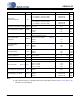
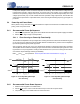
ELECTRICAL CHARACTERISTICS - FHD MODE
Note:
13. SNR
A
dB is referenced to the output signal amplitude resulting in the specified output power at
THD+N < 1 %. See “Parameter Definitions” on page 29 for more information.
14. Idle Current Draw (I
IDLE
) is specified without any output filtering. Refer to Section 5.3 on page 17 for
information on output filtering. At idle, the output devices will switch at the same rate in HD and FHD
mode. FHD only changes the output switching frequency when the input levels are above the “Input
Level for Entering VBATT Operation in HD/FHD Modes (V
IN-VBATT
) given in “Electrical Characteristics
- All Operational Modes” on page 9.
Parameters Symbol Test Conditions Min Typ Max Units
Output Power
(Continuous Average)
P
O
THD+N = 1%
R
L
= 8 (VBATT = 5.0/4.2/3.7 VDC)
R
L
= 4 (VBATT = 5.0/4.2/3.7 VDC)
-
-
1.33/0.94/0.72
2.31/1.63/1.23
-
-
W
W
THD+N = 10%
R
L
= 8 (VBATT = 5.0/4.2/3.7 VDC)
R
L
= 4 (VBATT = 5.0/4.2/3.7 VDC)
-
-
1.71/1.21/0.94
2.95/2.09/1.61
-
-
W
W
Total Harmonic Distortion + Noise THD+N
P
O
= 1.0 W - 0.11 - %
Power Supply Rejection Ratio PSRR
V
ripple
= 200 mV
PP
, AINx AC coupled to GND
@ 217 Hz
@ 1 kHz
-
-
89
85
-
-
dB
dB
Common-Mode Rejection Ratio CMRR
V
ripple
=1V
PP
, f
ripple
= 217 Hz
-71-dB
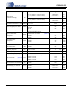
Signal to Noise Ratio
A-Weighted
SNR
A
Inputs AC Coupled to Ground,
Referenced to 1% THD+N (Note 13)
CS35L03
CS35L01
-
-
93
94
-
-
dB
dB
Idle Channel Noise
A-Weighted
ICN
A
AIN+ connected to AIN-
CS35L03
CS35L01
-
-
71
63
-
-
Vrms
Vrms
Idle Channel Noise ICN
AIN+ connected to AIN-
CS35L03
CS35L01
-
-
125
115
-
-
Vrms
Vrms
Frequency Response FR 20 Hz to 20 kHz -4.0 0 0.5 dB
Output Switching Frequency
f
sw1
LDO Operation - 192 - kHz
Total Group Delay GD - 14 - s
Output Switching Frequency
f
sw2
VBATT Operation
- 76 - kHz
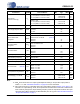
Idle Current Draw (Note 14) I
IDLE
AIN+ connected AIN-, No Output Load
VBATT = 5.0 VDC
VBATT = 4.2 VDC
VBATT = 3.7 VDC
-
-
-
1.09
1.04
1.01
-
-
-
mA
mA
mA
Input Impedance, Single Ended
Z
IN
CS35L03
CS35L01
-
-
160
240
-
-
k
k
Input Voltage @ 1 % THD+N V
ICLIP
R
L
= 8 (VBATT = 5.0/4.2/3.7 VDC)
CS35L03
CS35L01
-
-
0.83/0.70/0.62
1.66/1.39/1.22
-
-
Vrms
Vrms