
User guide
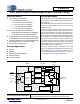

CS35L00
DS906PP1 9
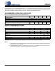
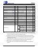
ELECTRICAL CHARACTERISTICS - ALL OPERATIONAL MODES
Note:
6. No external loads should be connected to the LFILT+ net. Any connection of a load to this point may
result in errant operation or performance degradation in the device.
7. When VBATT is below this threshold (VB
LIM
), operation is automatically restricted to SD mode.
8. When operating in HD or FHD mode and the differential input voltage remains below the input level
threshold (V
IN-LDO
) for a period of time (t
LDO
), the PWM outputs will be powered by the internally
generated LDO supply (VLDO).
9. When operating in HD or FHD mode and the differential input voltage is above this input level
threshold (V
IN-VBATT
), the PWM outputs will be powered directly from the VBATT supply.
10. Refer to Section 5.5 for more information on Thermal Error functionality.
11. Under Voltage Lockout is the threshold at which a decreasing VBATT supply will disable device
operation.
Parameters Symbol Test Conditions Min Typ Max Units
Max. Current from LFILT+ (Note 6)
I
LFILT+
-10 -μA
LFILT+ Output Impedance Z
LFILT+
-0.7 -Ω
VBATT Limit for HD/FHD Mode (Note 7)
VB
LIM
-3.0 -VDC
Input Level for Entering LDO Operation in
HD/FHD Modes (Note 8)
V
IN-LDO
GAIN_SEL = Low (12 dB)
GAIN_SEL = High (6 dB)
-
-
0.015•VBATT
0.029•VBATT
-
-
Vrms
Vrms
Input Level for Entering VBATT Operation in
HD/FHD Modes (Note 9)
V
IN-VBATT
GAIN_SEL = Low (12 dB)
GAIN_SEL = High (6 dB)
-
-
0.10
0.20
-
-
Vrms
Vrms
LDO Entry Time Delay
t
LDO
- 1200 - ms
LDO Level for HD/FHD Modes VLDO - 1.0 - V
Output Offset Voltage
V
OFFSET
Inputs AC coupled to GND
-+/-2 -mV
Amplifier Gain
A
V
GAIN_SEL = Low
GAIN_SEL = High
-
-
12
6
-
-
dB
dB
Shutdown Supply Current I
A(SD)
SD = Low
-0.05 -μA
MOSFET On Resistance R
DS(ON)
I
bias
= 0.5 A
-350 -mΩ
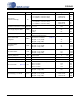
Thermal Error Threshold (Note 10)
T
TE
-150 -°C
Thermal Error Retry Time (Note 10)
R
TE
- 1200 - ms
Under Voltage Lockout Threshold (Note 10)
UVLO - 2.0 - V
Operating Efficiency η
Output Levels at 10% THD+N
8 Ω + 33μH
Load
VBATT = 5 VDC - 90 - %
VBATT = 3.7 VDC - 89 - %
4 Ω + 33μH
Load
VBATT = 5 VDC - 84 - %
VBATT = 3.7 VDC - 83 - %