
User guide

CS35L00
DS906PP1 33
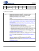
9. ORDERING INFORMATION
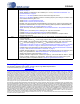
10.REVISION HISTORY
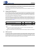
Product Description Package Pb-Free Grade Temp Range Container Order#
CS35L00 2.8 W Mono Audio
Amplifier with select-
able gain
10-DFN Yes Commercial -10° to +70°C Rail CS35L00-CNZ
Tape and Reel CS35L00-CNZR
Release Changes
A1 Initial Release
A2 – Updated all output switching frequency references to f
sw1
from 200 kHz to 192 kHz.
– Updated all output switching frequency references to f
sw2
from 80 kHz to 76 kHz.
– Updated front page title, features, and common applications.
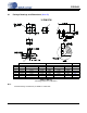
– Updated front page block diagram.
– Updated Section 3. Typical Connection Diagrams to show 10
μF and 0.1 μF power-supply decoupling
capacitors.
– Reorganized location of individual specifications in electrical characteristics tables based on measured
device performance in different operational modes (“Electrical Characteristics - All Operational Modes”
on page 9, “Electrical Characteristics - SD Mode” on page 10, “Electrical Characteristics - FSD Mode”
on page 11, “Electrical Characteristics - HD Mode” on page 12, and “Electrical Characteristics - FHD
Mode” on page 13).
– The following specification changes have been made in “Electrical Characteristics - SD Mode” on
page 10, “Electrical Characteristics - FSD Mode” on page 11, “Electrical Characteristics - HD Mode” on
page 12, and “Electrical Characteristics - FHD Mode” on page 13:
– Added “Common-Mode Rejection Ratio” test conditions (V
ripple
=1V
PP
and f
ripple
= 217 Hz)
– Updated “Signal to Noise Ratio” to be specified as A-Weighted
– Updated “Idle Channel Noise” to be specified as both A-Weighted & Unweighted
– Updated “Idle Current Draw” to be specified with no load at 3 voltages (5.0 V, 4.2 V, and 3.7 V)
– Changed “Max Input Before Clipping specification to “Input Voltage @ 1 % THD+N”
– Updated specification typical values for 1% Output Power, 10% Output Power, THD+N @ 1 W, SNR
A-Weighted, Idle Channel Noise A-Weighted, Idle Channel Noise (unweighted), Frequency
Response, Output Switching Frequency, Input Impedance, and Input Voltage @ 1% THD+N
– Updated “Operating Efficiency” to be specified with 8 Ω + 33
μH and 4 Ω + 33 μH in “Electrical
Characteristics - All Operational Modes” on page 9.
– Modified “Power-Up Time” specification into “Start-Up Time” and “Zero Crossing Power-Up” and added
a cross-reference in “Power-Up & Power-Down Characteristics” on page 14.
– Moved power-up and power-down timing specifications from “Electrical Characteristics - All Operational
Modes” on page 9 to their own specification table, “Power-Up & Power-Down Characteristics” on
page 14.
– Renamed “Thermal Error Wait Time (W
TE
)” to “Thermal Error Retry Time (R
TE
)” in “Electrical
Characteristics - All Operational Modes” on page 9 and in Section 5.5 Over Temperature Protection and
added (Note 10) Thermal Error cross reference from spec table to description section.
– Updated “Operating Efficiency” specification (η) in “Electrical Characteristics - All Operational Modes”
on page 9.
– Updated “MOSFET On Resistance” specification (R
DS(ON)
) in “Electrical Characteristics - All
Operational Modes” on page 9.