
User guide

CS35L00
14 DS906PP1
DIGITAL INTERFACE SPECIFICATIONS & CHARACTERISTICS
POWER-UP & POWER-DOWN CHARACTERISTICS
Note:
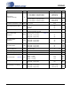
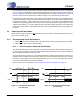
15. Start-Up Time (t
start
) refers to the internal start-up time from when SD is released to when the device
is ready to activate the PWM outputs. The total power-up time from SD
release to the PWM outputs
becoming active will vary based on the input signal, not exceeding the Start-Up Time + Zero Crossing
Power-Up Timeout (t
start
+t
timeout
). For more information refer to Section 5.4.
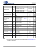
Parameters Symbol Min Max Units
Input Leakage Current I
in
-±10μA
Input Capacitance -10pF
SD Pulse Width Requirement 1 - ms
Logic I/Os (Applicable to GAIN_SEL, MODE, and SD
)
High-Level Input Voltage V
IH
0.7•VBATT - V
Low-Level Input Voltage V
IL
- 0.3•VBATT V
Parameters Symbol Test Conditions Min Typ Max Units
Start-Up Time (Note 15)
t
start
After “Low” to “High” SD Pin transition edge
-18-ms
Zero Crossing Power-Up Timeout
t
timeout
No audio input applied
-25-ms
Power-Down Time
t
off
After “High” to “Low” SD Pin transition edge
-1-ms