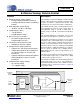
CS3308 8-Channel Analog Volume Control Features Description Complete Analog Volume Control – – 8 Independently Controllable Channels 3 Configurable Master Volume and Muting Controls Wide Adjustable Volume Range – The CS3308 includes arrays of well-matched resistors and complementary low-noise active output stages. A total adjustable range of 118 dB, in ¼ dB steps, is spread evenly over 96 dB of attenuation and 22 dB of gain.
CS3308 TABLE OF CONTENTS 1. PIN DESCRIPTIONS ............................................................................................................................ 5 2. CHARACTERISTICS AND SPECIFICATIONS .................................................................................... 7 SPECIFIED OPERATING CONDITIONS .................................................................................................... 7 ABSOLUTE MAXIMUM RATINGS.........................................................
CS3308 7.4.2 MUTE Input Polarity (Bit 4) ................................................................................................ 33 7.4.3 Channel B = Channel A (Bit 0 - 3) ..................................................................................... 34 7.5 Device Configuration 2 - Address 0Ch ........................................................................................ 34 7.5.1 Zero-Crossing Time-Out Period (Bits 4:2) ..............................................................
CS3308 LIST OF FIGURES Figure 1.Control Port Timing - I²C Format.................................................................................................. 10 Figure 2.Control Port Timing - SPI Format................................................................................................. 11 Figure 3.Typical Connection Diagram........................................................................................................ 12 Figure 4.Detailed Block Diagram .............................
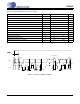
CS3308 OUT3 REFO3 IN3 REFI3 REFI2 IN2 REFO2 OUT2 VA+ VA- OUT1 REFO1 1.
CS3308 Pin Name # OUT1 47 OUT2 44 OUT3 37 OUT4 34 OUT5 27 OUT6 24 OUT7 17 OUT8 14 REFI1 2 REFI2 41 REFI3 40 REFI4 31 REFI5 30 REFI6 21 REFI7 20 REFI8 11 REFO1 48 REFO2 43 REFO3 38 REFO4 33 REFO5 28 REFO6 23 REFO7 18 REFO8 13 Pin Description Analog Outputs (Output) - The full-scale output level is specified in the Analog Characteristics specification table. Reference In (Input) - Analog reference pin. Reference Out (Output) - Analog reference pin.
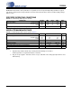
CS3308 2. CHARACTERISTICS AND SPECIFICATIONS All Min/Max characteristics and specifications are guaranteed over the Specified Operating Conditions. Typical performance characteristics and specifications are derived from measurements taken at nominal supply voltages and TA = 25°C. SPECIFIED OPERATING CONDITIONS (DGND = 0 V; All voltages with respect to ground.
CS3308 ANALOG CHARACTERISTICS (Test conditions (unless otherwise specified): RS = 0; RL = 2 kΩ; CL = 20 pF; 10 Hz to 20 kHz Measurement Bandwidth) Parameter Symbol Min Typ Max Unit RIN CIN 8 - 0.25 ±0.5 ±0.1 10 10 - dB dB dB kΩ pF 117 (VA-) + 1.35 - 0.00025 123 1.8 -120 VOS ROUT RLOAD 2 - 0.75 100 20 5 5 100 - mV Ω kΩ pF mA MHz IVA+ IVAIVD IPD - 36 36 0.6 60 362 300 80 50 50 1.
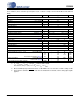
CS3308 DIGITAL INTERFACE CHARACTERISTICS Parameters Symbol Min Typ Max Units High-Level Input Voltage Low-Level Input Voltage High-Level Output Voltage at Io=2 mA VIH VIL VOH 0.7 x VD VD - 1.0 - 0.2 x VD - V V V Low-Level Output Voltage at Io=2 mA VOL - - 0.4 V Iin - 8 ±10 - μA pF Symbol Min Typ Max Units - 2 - - ms Input Leakage Current Input Capacitance MUTE SWITCHING CHARACTERISTICS (Inputs: Logic 0 = DGND, Logic 1 = VD) Parameters MUTE Active Pulse Width (Note 6) 6.
CS3308 CONTROL PORT SWITCHING CHARACTERISTICS - I²C FORMAT (Inputs: Logic 0 = DGND, Logic 1 = VD, CL = 20 pF) Symbol Min Max Unit SCL Clock Frequency Parameter fscl - 100 kHz RESET Rising Edge to Start tirs 100 - ns Bus Free Time Between Transmissions tbuf 4.7 - µs Start Condition Hold Time (prior to first clock pulse) thdst 4.0 - µs Clock Low time tlow 4.7 - µs Clock High Time thigh 4.0 - µs Setup Time for Repeated Start Condition tsust 4.
CS3308 CONTROL PORT SWITCHING CHARACTERISTICS - SPI™ FORMAT (Inputs: Logic 0 = DGND, Logic 1 = VD, CL = 20 pF) Parameter Symbol Min Max Unit CCLK Clock Frequency fsck 0 6.0 MHz RESET Rising Edge to CS Falling tsrs 100 - ns CS High Time Between Transmissions tcsh 1.
CS3308 3. TYPICAL CONNECTION DIAGRAM +5 V +5 V 10 µF 0.1 µF 0.1 µF 10 µF Audio Source 36 + VA - 35 VA VA 45 VA 46 + -5 V - -5 V 1 IN1 OUT1 47 42 IN2 OUT2 44 39 IN3 OUT3 37 32 IN4 OUT4 34 29 IN5 OUT5 27 22 IN6 OUT6 24 19 IN7 12 IN8 CS3308 Audio Outputs OUT7 17 OUT8 14 See Note 2 kΩ 5 6 SDA/MOSI 7 AD0/CS 3 RESET 4 MUTE +3.3 V VD 10 0.
CS3308 4.
CS3308 5. APPLICATIONS 5.1 General Description The CS3308 is an 8-channel digitally controlled analog volume control designed for audio systems. It incorporates a total adjustable range of 118 dB in ¼ dB steps, spread evenly over 96 dB of attenuation and 22 dB of gain. The internal analog architecture includes one op-amp per channel, each with an input resistor network for attenuation and a feedback resistor network for gain.
CS3308 5.2.2 Analog Outputs The analog outputs are capable of driving 2 kΩ loads to within 1.35 V of the analog supply rails and are short-circuit protected to 20 mA. The minimum output load resistance is 2 kΩ; a load smaller than 2 kΩ may cause increased distortion. As the load resistance decreases, the potential for increased internal heating and the possibility of damage to the device is introduced. Additionally, the load capacitance should be less than 100 pF.
CS3308 5.3.1 Recommended Power-Up Sequence 1. Hold RESET low until the power supplies are stable. In this state, the control port is reset to its default settings. 2. Bring RESET high. The device will remain in a low power state with the PDN_ALL bit set by default. The control port will be accessible. 3. The desired register settings can be loaded while the PDN_ALL bit remains set. 4. Clear the PDN_ALL bit to initiate the power-up sequence. 5.3.2 Recommended Power-Down Sequence 1.
CS3308 5.4 Volume & Muting Control Architecture The CS3308’s volume and muting control architecture provides the ability to control each channel on an individual and master basis. Individual control allows the volume and mute state of a single channel to be changed independently from all other channels within the device. The CS3308 provides 8 individual volume and muting controls, each permanently assigned to one channel within the device.
CS3308 Combining the multiple group addressing capabilities of the CS3308 (as detailed in section 5.8.2 on page 24) with the internal master control mapping abilities described above allows the configuration and direct addressing of multiple logical groups of channels across multiple CS3308 devices within a system. Referenced Control Register Location Master X Mask ....................
CS3308 5.5 Volume Controls The CS3308 provides comprehensive volume control functionality, allowing each channel’s volume to be changed on an individual or master basis. Refer to the “Volume & Muting Control Architecture” section on page 17 for complete details about the configuration of the CS3308’s individual and master controls.
CS3308 Table 1 shows example volume settings using individual and master volume controls. IndividualChX Master 1 Channel 1 +3.75 dB Mask 1ChX Master 2 Mask 2ChX 0 Master 3 0 Mask 3ChX LevelChX 0 +3.75 dB Channel 2 +2.5 dB 0 0 1 -6.0 dB Channel 3 +1.25 dB 0 1 0 +6.5 dB Channel 4 0 dB Channel 5 -1.25 dB +1.0 dB 0 1 +5.25 dB 1 0 -8.5 dB 1 -3.25 dB 0 -0.25 dB Channel 6 -2.5 dB 1 0 1 -10.0 dB Channel 7 -3.75 dB 1 1 0 +2.5 dB Channel 8 -4.0 dB 1 1 1 -6.
CS3308 5.6 Muting Controls The CS3308 provides flexible muting capabilities to complement its comprehensive volume control abilities. Each channel’s mute state may be controlled on an individual channel basis, by any of 3 master mute controls, and by the hardware MUTE input pin. The mute state of any channel within the CS3308 is determined by the logical OR of four conditions, and the channel will mute if any one or more of the conditions are met. These conditions are: 1. 2. 3. 4.
CS3308 5.7 Zero-Crossing Detection The CS3308 incorporates comprehensive zero-crossing detection features to provide for noise-free level transitions. Three zero-crossing detection modes and 8 selectable time-out periods are available for enhanced flexibility. Zero-crossing detection and time-out is implemented independently for each channel. 5.7.1 Zero-Crossing Modes The zero-crossing mode for all channels within the CS3308 are configured via the ZCMode[1:0] bits in the Device Config 2 register.
CS3308 5.8 System Serial Control Configuration The CS3308 includes a comprehensive serial control port which supports both SPI and I²C modes of communication (See the “I²C/SPI Serial Control Formats” section on page 27). The control port uses the shared serial control bus to define each device’s slave address. This allows independent control of up to 128 devices on the shared serial control bus without requiring hardware device address configuration pins or any more than one CS signal (for SPI mode).
CS3308 5.8.2 Serial Control within a Multiple-CS3308 System The CS3308 allows both independent and simultaneous control of up to 128 devices on a shared I²C or SPI serial control bus. The address of each device is configured by the host controller via the shared serial control bus. All serial communication, including the configuration of each device’s address, adheres to a standard I²C or SPI bus protocol.
CS3308 input of device N+1 may be repeated for up to 128 devices per single CS signal. If more than 128 devices are required in a system, separate CS signals may be used to create additional chains of up to 128 devices per CS signal. As each device is placed into reset (RESET is low), its ENOut signal is driven low.
CS3308 Once this configuration process is complete, every device may be independently controlled with a standard SPI communication cycle using the device’s newly assigned Individual device addresses. 5.8.2.2 I²C Mode Control Configuration Up to 128 CS3308’s may be connected to a common I²C serial control bus. This shared serial bus is used to assign a unique device address to each device on the bus such that they may be independently addressed.
CS3308 5.9 I²C/SPI Serial Control Formats The control port is used to access the internal registers of the CS3308. The control port has 2 modes: SPI and I²C, with the CS3308 acting as a slave device. SPI Mode is selected if there is a high-to-low transition on the CS pin after the RESET pin has been brought high. I²C Mode is selected by connecting the CS pin to VD or DGND. 5.9.1 I²C Mode In I²C Mode, SDA is a bidirectional data line. Data is clocked into and out of the CS3308 by the clock, SCL.
CS3308 0 1 2 3 4 5 6 7 8 9 10 11 12 13 14 15 16 17 18 19 20 21 22 23 24 25 26 27 28 SCL CHIP ADDRESS (WRITE) SDA MSB Chip Address LSB STOP MAP BYTE 0 INCR 6 5 4 3 2 1 CHIP ADDRESS (READ) 0 ACK MSB Chip Address LSB ACK START DATA 7 1 ACK DATA +1 0 7 ACK START 0 DATA + n 7 0 NO ACK STOP Figure 13. Control Port Timing, I²C Read Since the read operation cannot set the MAP, an aborted write operation is used as a preamble.
CS3308 6. CS3308 REGISTER QUICK REFERENCE This table shows the register names and their associated default values. Addr Function 01h Ch. 1 Volume page 31 02h Ch. 2 Volume page 31 03h Ch. 3 Volume page 31 04h Ch. 4 Volume page 31 05h Ch. 5 Volume page 31 06h Ch. 6 Volume page 31 07h Ch. 7 Volume page 31 08h Ch.
CS3308 Addr Function 10h Master 1 Mask page 36 11h Master 1 Volume page 36 12h Master 1 Control page 37 13h Master 2 Mask page 37 14h Master 2 Volume page 37 15h Master 2 Control page 38 16h Master 3 Mask page 38 17h Master 3 Volume page 38 18h Master 3 Control page 39 19h Group 2 Chip Addr page 40 1Ah Group 1 Chip Addr page 40 1Bh Individual Chip Addr page 41 1Ch Chip ID page 41 30 7 M1_Ch8M 6 5 M1_Ch7M M1_Ch6M 4 M1_Ch5M 3 2 1 0 M1_Ch4M M1_Ch3M M1_Ch2M M1_Ch1M 1 1 1 1 1 1 1 1 M1_Vol7
CS3308 7. CS3308 REGISTER DESCRIPTIONS Notes: 1. When addressing the CS3308 with the Individual Chip Address, all registers are read/write in I²C Mode and write-only in SPI Mode, unless otherwise noted. 2. When addressing the CS3308 with the Group Chip Addresses, all registers are write-only in both I²C and SPI Mode. 7.1 Ch 1-8 Volume - Addresses 01h - 08h 7 Vol7 7.1.
CS3308 7.2 ¼ dB Control - Address 09h 7 Quarter8 7.2.1 6 Quarter7 5 Quarter6 4 Quarter5 3 Quarter4 2 Quarter3 1 Quarter2 0 Quarter1 ¼ dB Control (Bit 0 - 7) Default = 0 Function: When set, ¼ dB of gain will be added to each bit’s respective channel. The volume changes are implemented as dictated by the ZCMode[1:0] and TimeOut[2:0] bits in the Device Config 2 register (see “Device Configuration 2 - Address 0Ch” on page 34).
CS3308 7.3 Mute Control - Address 0Ah 7 MuteCh8 7.3.1 6 MuteCh7 5 MuteCh6 4 MuteCh5 3 MuteCh4 2 MuteCh3 1 MuteCh2 0 MuteCh1 Mute Channel X (Bit 0 - 7) Default = 0 Function: Each bit controls the individual mute state of its respective channel. When set, the mute condition is active. When cleared, the mute condition is released. See “Muting Controls” on page 21 for more information about the muting behavior of the CS3308. 7.4 Device Configuration 1 - Address 0Bh (Bit 5) 7 Reserved 7.4.
CS3308 7.4.3 Channel B = Channel A (Bit 0 - 3) Default = 0 Function: When this bit is set, Channel A and Channel B volume levels and muting conditions are controlled by the Channel A volume and muting register settings, and the Channel B register settings are ignored. When this bit is cleared, Channel A and Channel B volume and mute settings are independently controlled by the A and B volume and muting bits.
CS3308 7.5.2 Zero-Crossing Mode (Bits 1:0) Default = 01 Function: These bits control the Zero-Crossing detection mode as shown in Table 9. Refer to the “Zero-Crossing Modes” section on page 22 for more information. ZCMode[1:0] Zero-Crossing Mode 00 Volume changes take effect immediately. 01 Volume changes take effect on a signal zero-crossing.
CS3308 7.8 Freeze Control - Address 0Fh 7 Reserved 7.8.1 6 Reserved 5 Reserved 4 Reserved 3 Reserved 2 Reserved 1 Reserved 0 Freeze Freeze (Bit 7) Default = 0 Function: When the Freeze bit is set, the Freeze function allows modifications to the control port registers without changes taking effect until Freeze bit is cleared. To make multiple changes in the Control Port registers take effect simultaneously, set the Freeze bit, make all register changes, then clear the Freeze bit. 7.
CS3308 7.11 Master 1 Control - Address 12h 7 Reserved 7.11.1 6 Reserved 5 Reserved 4 Reserved 3 Reserved 2 Reserved 1 M1_Mute 0 M1_Qtr Master 1 Mute (Bit 1) Default = 0 Function: This bit controls the Master 1 mute state. When set, the Master 1 mute condition is active. When cleared, the Master 1 mute condition is released. See “Muting Controls” on page 21 for more information about the muting behavior of the CS3308. 7.11.
CS3308 In the equation above, “Desired Volume Setting in dB” is determined by rounding the desired ¼ dB resolution volume setting down to ½ dB resolution. It should be noted that input values outside the CS3308’s analog range of +22 dB to -96 dB are valid; however, the volume of each channel will be limited to the CS3308’s analog range (see “Volume Limits” on page 20). See Table 5 on page 31 for example register settings. 7.
CS3308 as dictated by the ZCMode[1:0] and TimeOut[2:0] bits in the Device Config 2 register (see “Device Configuration 2 - Address 0Ch” on page 34). The value of the Master 3 volume control register is mapped to the desired 0.5 dB step Master 3 volume setting by the following equation: Register Value = ( 2 × Desired Volume Setting in dB ) + 210 In the equation above, “Desired Volume Setting in dB” is determined by rounding the desired ¼ dB resolution volume setting down to ½ dB resolution.
CS3308 7.18 Group 2 Chip Address 19h 7 G2_Addr6 6 G2_Addr5 5 G2_Addr4 4 G2_Addr3 3 G2_Addr2 2 G2_Addr1 1 G2_Addr0 0 EnG2Addr 7.18.1 Group 2 Chip Address (Bits 7:1) SPI Mode Default = 1000000b I²C Mode Default = See Table 4 on page 27. Function: These bits set the Group 2 chip address, and may be modified at any time. See “System Serial Control Configuration” on page 23 and “I²C/SPI Serial Control Formats” on page 27 for more information. 7.18.
CS3308 7.20 Individual Chip Address 1Bh 7 Ind_Addr6 6 Ind_Addr5 5 Ind_Addr4 4 Ind_Addr3 3 Ind_Addr2 2 Ind_Addr1 1 Ind_Addr0 0 Enable 7.20.1 Individual Chip Address (Bits 7:1) SPI Mode Default = 1000000b I²C Mode Default = See Table 4 on page 27 Function: These bits set the individual chip address, and may be modified at any time. See “System Serial Control Configuration” on page 23 and “I²C/SPI Serial Control Formats” on page 27 for more information. 7.20.
CS3308 8. PARAMETER DEFINITIONS Dynamic Range Full-scale (RMS) signal to broadband noise ratio. The broadband noise is measured over the specified bandwidth with the input grounded. Expressed in decibels. Total Harmonic Distortion + Noise The ratio of the rms value of the signal to the rms sum of all other spectral components over the specified bandwidth (typically 10 Hz to 20 kHz), including distortion components. Expressed in decibels.
CS3308 9. PACKAGE DIMENSIONS 48L LQFP PACKAGE DRAWING E E1 D D1 1 e B ∝ A A1 L DIM A A1 B D D1 E E1 e* L MIN --0.002 0.007 0.343 0.272 0.343 0.272 0.016 0.018 0.000° ∝ * Nominal pin pitch is 0.50 mm INCHES NOM MAX MIN 0.055 0.063 --0.004 0.006 0.05 0.009 0.011 0.17 0.354 0.366 8.70 0.28 0.280 6.90 0.354 0.366 8.70 0.28 0.280 6.90 0.020 0.024 0.40 0.24 0.030 0.45 4° 7.000° 0.00° *Controlling dimension is mm. MILLIMETERS NOM MAX 1.40 1.60 0.10 0.15 0.22 0.27 9.0 BSC 9.30 7.0 BSC 7.10 9.0 BSC 9.30 7.
CS3308 11.ORDERING INFORMATION Product CS3308 CDB3308 Description Package 8-Channel 48-pin Analog Volume Control LQFP CS3308 Evaluation Board Pb-Free Grade Temp Range YES Commercial -10° to +70° C No - - Container Order # Tray CS3308-CQZ Tape & Reel CS3308-CQZR CDB3308 12.REVISION HISTORY Release A1 PP1 F1 Changes Initial Release of Advance Datasheet Initial Release of Preliminary Datasheet – Updated THD+N shown on cover page.