
User Manual

CS3013
4 DS736F3
10/15/09
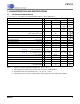
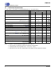
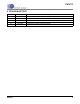
1.2 3 V Electrical Characteristics
V+ = +3 V,
±10%;
V- = 0V; VCM = 1.5 V; Unless otherwise noted,
T
A
= 25º C (See Note 5).
Notes: 5. Symbol “•” denotes specification applies over -40 to +125
° C.
6. This parameter is guaranteed by design and laboratory characterization.
7. Guaranteed within the output limits of (V+ – 0.2 V) to (V- + 0.2 V).
8. Specifies the worst case drive voltage relative to the supply rail under stated load conditions.
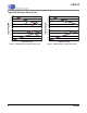
Parameter Min Typ Max Unit
Input Offset Voltage (Note 6) • -±10±20µV
Average Input Offset Drift (Note 6) • - ±0.01 ±0.05 µV/ºC
Input Bias Current
•
-
-
±110
-
±150
±1.0
pA
nA
Input Offset Current
•
-
-
±220
-
±300
±2.0
pA
nA
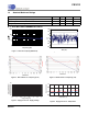
Input Noise Voltage Density R
S
= 100 Ω, f
0
= 1 Hz
R
S
= 100 Ω, f
0
= 1 kHz
-
-
22
22
-
-
Input Noise Voltage 0.1 to 10 Hz - 460 - nV
p-p
Input Noise Current Density f
0
= 1 Hz - 100 -
Input Noise Current 0.1 to 10 Hz - 1.9 - pA
p-p
Input Voltage Range (Note 6) • V- - V+ V
Common Mode Rejection Ratio (dc) • 105 120 - dB
Power Supply Rejection Ratio • 100 120 - dB
Large Signal Voltage Gain
(Note 7)R
L
= 2 kΩ to V+/2 •
-
112
145
135
-
-
dB
dB
Output Voltage Swing R
L
= 2 kΩ to V+/2
(Note 8)R
L
= 100 kΩ to V+/2
• (V+ – 200)
(V+ – 20)
-
-
(V- + 200)
(V- + 20)
mV
mV
Slew Rate R
L
= 2 k, 100 pF - 0.25 - V/µs
Overload Recovery Time - 40 - µs
Supply Current • - 1.0 1.25 mA
Chopping Frequency - 125 - kHz
Input Capacitance Differential
Common Mode
-
-
1.5
10
-
-
pF
pF
nV/ Hz
nV/ Hz
fA/ Hz