
Manual

CS2300-CP
4 DS843F2
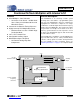
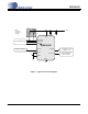
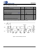
1. PIN DESCRIPTION
Pin Name # Pin Description
VD 1 Digital Power (Input) - Positive power supply for the digital and analog sections.
GND 2 Ground (Input) - Ground reference.
CLK_OUT 3 PLL Clock Output (Output) - PLL clock output.
AUX_OUT
4 Auxiliary Output (Output) - This pin outputs a buffered version of one of the input or output clocks,
or a status signal, depending on register configuration.
CLK_IN 5 Frequency Reference Clock Input (Input) - Clock input for the Digital PLL frequency reference.
FILTP
FILTN
6
7
LCO Filter Connections (Input/Output) - These pins provide external supply filtering for the inter-
nal LC Oscillator.
AD0/CS
8 Address Bit 0 (I²C) / Control Port Chip Select (SPI) (Input) - AD0 is a chip address pin in I²C
Mode. CS is the chip select signal in SPI Mode.
SCL/CCLK
9 Control Port Clock (Input) - SCL/CCLK is the serial clock for the serial control port in I²C and SPI
mode.
SDA/CDIN
10 Serial Control Data (Input/Output) - SDA is the data I/O line in I²C Mode. CDIN is the input data
line for the control port interface in SPI Mode.
1
2
3
4
5
6
7
8
9
10
FILTP
CLK_OUT
GND
VD
FILTN
AD0/CS
SCL/CCLK
SDA/CDIN
AUX_OUT
CLK_IN