
Manual

CS2300-CP
2 DS843F2
TABLE OF CONTENTS
1. PIN DESCRIPTION ................................................................................................................................. 5
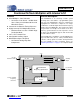
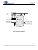
2. TYPICAL CONNECTION DIAGRAM ..................................................................................................... 6
3. CHARACTERISTICS AND SPECIFICATIONS ...................................................................................... 7
RECOMMENDED OPERATING CONDITIONS .................................................................................... 7
ABSOLUTE MAXIMUM RATINGS ........................................................................................................ 7
DC ELECTRICAL CHARACTERISTICS ................................................................................................ 7
AC ELECTRICAL CHARACTERISTICS ................................................................................................ 8
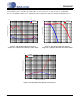
PLL PERFORMANCE PLOTS ............................................................................................................... 9
CONTROL PORT SWITCHING CHARACTERISTICS- I²C FORMAT ................................................. 10
CONTROL PORT SWITCHING CHARACTERISTICS - SPI FORMAT ............................................... 11
4. ARCHITECTURE OVERVIEW ............................................................................................................. 12
4.1 Delta-Sigma Fractional-N Frequency Synthesizer ......................................................................... 12
4.2 Hybrid Analog-Digital Phase Locked Loop ....................................................................................12
5. APPLICATIONS ................................................................................................................................... 14
5.1 Timing Reference Clock ................................................................................................................. 14
5.2 Frequency Reference Clock Input, CLK_IN ................................................................................... 14
5.2.1 CLK_IN Skipping Mode ......................................................................................................... 14
5.2.2 Adjusting the Minimum Loop Bandwidth for CLK_IN ............................................................ 16
5.3 Output to Input Frequency Ratio Configuration ............................................................................. 17
5.3.1 User Defined Ratio (RUD) ..................................................................................................... 17
5.3.2 Ratio Modifier (R-Mod) .......................................................................................................... 18
5.3.3 Effective Ratio (REFF) .......................................................................................................... 18
5.3.4 Ratio Configuration Summary ............................................................................................... 19
5.4 PLL Clock Output ........................................................................................................................... 20
5.5 Auxiliary Output .............................................................................................................................. 20
5.6 Clock Output Stability Considerations ............................................................................................ 21
5.6.1 Output Switching ................................................................................................................... 21
5.6.2 PLL Unlock Conditions .......................................................................................................... 21
5.7 Required Power Up Sequencing .................................................................................................... 21
6. SPI / I²C CONTROL PORT ................................................................................................................... 21
6.1 SPI Control ..................................................................................................................................... 22
6.2 I²C Control ...................................................................................................................................... 22
6.3 Memory Address Pointer ............................................................................................................... 24
6.3.1 Map Auto Increment .............................................................................................................. 24
7. REGISTER QUICK REFERENCE ........................................................................................................ 24
8. REGISTER DESCRIPTIONS ................................................................................................................ 25
8.1 Device I.D. and Revision (Address 01h) ........................................................................................ 25
8.1.1 Device Identification (Device[4:0]) - Read Only ..................................................................... 25
8.1.2 Device Revision (Revision[2:0]) - Read Only ........................................................................ 25
8.2 Device Control (Address 02h) ........................................................................................................ 25
8.2.1 Unlock Indicator (Unlock) - Read Only .................................................................................. 25
8.2.2 Auxiliary Output Disable (AuxOutDis) ................................................................................... 25
8.2.3 PLL Clock Output Disable (ClkOutDis) .................................................................................. 26
8.3 Device Configuration 1 (Address 03h) ........................................................................................... 26
8.3.1 R-Mod Selection (RModSel[2:0]) ...........................................................................................26
8.3.2 Auxiliary Output Source Selection (AuxOutSrc[1:0]) ............................................................. 26
8.3.3 Enable Device Configuration Registers 1 (EnDevCfg1) ........................................................ 27
8.4 Global Configuration (Address 05h) ............................................................................................... 27
8.4.1 Device Configuration Freeze (Freeze) .................................................................................. 27
8.4.2 Enable Device Configuration Registers 2 (EnDevCfg2) ........................................................ 27
8.5 Ratio (Address 06h - 09h) .............................................................................................................. 27
8.6 Function Configuration 1 (Address 16h) ........................................................................................ 28