CS2300-CP Fractional-N Clock Multiplier with Internal LCO Features General Description Clock Multiplier / Jitter Reduction The CS2300-CP is an extremely versatile system clocking device that utilizes a programmable phase lock loop. The CS2300-CP is based on a hybrid analog-digital PLL architecture comprised of a unique combination of a Delta-Sigma Fractional-N Frequency Synthesizer and a Digital PLL.
CS2300-CP TABLE OF CONTENTS 1. PIN DESCRIPTION ................................................................................................................................. 5 2. TYPICAL CONNECTION DIAGRAM ..................................................................................................... 6 3. CHARACTERISTICS AND SPECIFICATIONS ...................................................................................... 7 RECOMMENDED OPERATING CONDITIONS .......................................
CS2300-CP 8.6.1 Clock Skip Enable (ClkSkipEn) ............................................................................................. 28 8.6.2 AUX PLL Lock Output Configuration (AuxLockCfg) .............................................................. 28 8.6.3 Enable Device Configuration Registers 3 (EnDevCfg3) ........................................................ 28 8.7 Function Configuration 2 (Address 17h) ........................................................................................
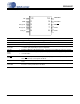
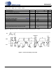
CS2300-CP 1. PIN DESCRIPTION VD 1 10 SDA/CDIN GND 2 9 SCL/CCLK CLK_OUT 3 8 AD0/CS AUX_OUT 4 7 FILTN CLK_IN 5 6 FILTP Pin Name # Pin Description VD 1 Digital Power (Input) - Positive power supply for the digital and analog sections. GND 2 Ground (Input) - Ground reference. CLK_OUT 3 PLL Clock Output (Output) - PLL clock output.
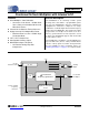
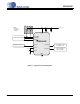
CS2300-CP 2. TYPICAL CONNECTION DIAGRAM Note1 Notes: 1. Resistors required for I2C operation. 0.1 µF 2 kΩ 1 µF +3.3 V 2 kΩ VD SCL/CCLK System MicroController SDA/CDIN AD0/CS CS2300-CP Frequency Reference CLK_IN 0.1 µF CLK_OUT To circuitry which requires a low-jitter clock AUX_OUT To other circuitry or Microcontroller FILTP FILTN GND Figure 1.
CS2300-CP 3. CHARACTERISTICS AND SPECIFICATIONS RECOMMENDED OPERATING CONDITIONS GND = 0 V; all voltages with respect to ground. (Note 1) Parameters DC Power Supply Symbol Min Typ Max Units VD 3.1 3.3 3.5 V TAC TAD -10 -40 - +70 +85 °C °C Ambient Operating Temperature (Power Applied) Commercial Grade Automotive Grade Notes: 1. Device functionality is not guaranteed or implied outside of these limits. Operation outside of these limits may adversely affect device reliability.
CS2300-CP AC ELECTRICAL CHARACTERISTICS Test Conditions (unless otherwise specified): VD = 3.1 V to 3.5 V; TA = -10°C to +70°C (Commercial Grade); TA = -40°C to +85°C (Automotive Grade); CL = 15 pF.
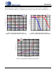
CS2300-CP PLL PERFORMANCE PLOTS Test Conditions (unless otherwise specified): VD = 3.3 V; TA = 25 °C; CL = 15 pF; fCLK_OUT = 12.288 MHz; fCLK_IN = 12.288 MHz; Sample size = 10,000 points; Base Band Jitter (100 Hz to 40 kHz); AuxOutSrc[1:0] = 11. 10,000 10 1 Hz Bandwidth 128 Hz Bandwidth 1 Hz Bandwidth 128 Hz Bandwidth 0 -10 Jitter Transfer (dB) Max Input Jitter Level (usec) 1,000 100 10 -20 -30 -40 1 -50 0.
CS2300-CP CONTROL PORT SWITCHING CHARACTERISTICS- I²C FORMAT Inputs: Logic 0 = GND; Logic 1 = VD; CL = 20 pF. Parameter Symbol Min Max Unit SCL Clock Frequency fscl - 100 kHz Bus Free-Time Between Transmissions tbuf 4.7 - µs Start Condition Hold Time (prior to first clock pulse) thdst 4.0 - µs Clock Low Time tlow 4.7 - µs Clock High Time thigh 4.0 - µs Setup Time for Repeated Start Condition tsust 4.
CS2300-CP CONTROL PORT SWITCHING CHARACTERISTICS - SPI FORMAT Inputs: Logic 0 = GND; Logic 1 = VD; CL = 20 pF. Parameter Symbol Min Max Unit fccllk - 6 MHz tspi 500 - ns CS High Time Between Transmissions tcsh 1.
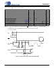
CS2300-CP 4. ARCHITECTURE OVERVIEW 4.1 Delta-Sigma Fractional-N Frequency Synthesizer The core of the CS2300 is a Delta-Sigma Fractional-N Frequency Synthesizer which has very high-resolution for Input/Output clock ratios, low phase noise, very wide range of output frequencies and the ability to quickly tune to a new frequency. The reference for the synthesizer is an on chip LC Oscillator (LCO) which generates the necessary internal stable clocks.
CS2300-CP Delta-Sigma Fractional-N Frequency Synthesizer LCO Phase Comparator Internal Loop Filter Voltage Controlled Oscillator PLL Output Fractional-N Divider Delta-Sigma Modulator Digital PLL and Fractional-N Logic N Digital Filter Frequency Reference Clock Frequency Comparator for Frac-N Generation Output to Input Ratio for Hybrid mode Figure 8.
CS2300-CP 5. APPLICATIONS 5.1 Timing Reference Clock The internal LC oscillator is used to generate the internal timing reference clock (see section 4 “Architecture Overview” on page 11 for information on how this internal clock is used by the CS2300). A single 0.1 µF cap must be connected between the FILTP and FILTN pins and the FILTN pin must be connected to ground as shown in Figure 9. FILTN FILTP C Figure 9. External Component Requirements for LCO 5.
CS2300-CP Regardless of the setting of the ClkSkipEn bit the PLL output will continue for 223 LCO cycles (518 ms to 634 ms) after CLK_IN is removed (see Figure 10). This is true as long as CLK_IN does not glitch or have an effective change in period as the clock source is removed, otherwise the PLL will interpret this as a change in frequency causing clock skipping and the 223 LCO cycle time-out to be bypassed and the PLL to immediately unlock.
CS2300-CP If CLK_IN is removed and then re-applied within tCS, the ClkSkipEn bit determines whether PLL_OUT continues while the PLL re-acquires lock (see Figure 12). When ClkSkipEn is disabled and CLK_IN is removed the PLL output will continue until CLK_IN is re-applied at which point the PLL will go unlocked only for the time it takes to acquire lock; the PLL_OUT state will be determined by the ClkOutUnl bit during this time.
CS2300-CP Typically, applications in which the PLL_OUT signal creates a new clock domain from which all other system clocks and associated data are derived will benefit from the maximum jitter and wander rejection of the lowest PLL bandwidth setting. See Figure 13. PLL BW = 1 Hz CLK_IN Wander > 1 Hz PLL_OUT Wander and Jitter > 1 Hz Rejected MCLK Jitter MCLK Subclocks generated from new clock domain. or LRCK LRCK SCLK SCLK D0 SDATA D1 SDATA D0 D1 Figure 13.
CS2300-CP in either a high resolution (12.20) or high multiplication (20.12) format selectable by the LFRatioCfg bit, with 20.12 being the default. The RUD for high resolution (12.20) format is encoded with 12 MSBs representing the integer binary portion with the remaining 20 LSBs representing the fractional binary portion. The maximum multiplication factor is approximately 4096 with a resolution of 0.954 PPM in this configuration. See “Calculating the User Defined Ratio” on page 29 for more information.
CS2300-CP Ratio modifiers which would produce an overflow or truncation of REFF should not be used; For example if RUD is 1024 an RMOD of 8 would produce an REFF value of 8192 which exceeds the 4096 limit of the 12.20 format. In all cases, the maximum and minimum allowable values for REFF are dictated by the frequency limits for both the input and output clocks as shown in the “AC Electrical Characteristics” on page 7. 5.3.
CS2300-CP 5.4 PLL Clock Output The PLL clock output pin (CLK_OUT) provides a buffered version of the output of the frequency synthesizer. The driver can be set to high-impedance with the ClkOutDis bit. The output from the PLL automatically drives a static low condition while the PLL is un-locked (when the clock may be unreliable). This feature can be disabled by setting the ClkOutUnl bit, however the state CLK_OUT may then be unreliable during an unlock condition.
CS2300-CP 5.6 Clock Output Stability Considerations 5.6.1 Output Switching CS2300 is designed such that re-configuration of the clock routing functions do not result in a partial clock period on any of the active outputs (CLK_OUT and/or AUX_OUT). In particular, enabling or disabling an output, and the automatic disabling of the output(s) during unlock will not cause a runt or partial clock period.
CS2300-CP The control port operates with either the SPI or I²C interface, with the CS2300 acting as a slave device. SPI Mode is selected if there is a high-to-low transition on the AD0/CS pin after power-up. I²C Mode is selected by connecting the AD0/CS pin through a resistor to VD or GND, thereby permanently selecting the desired AD0 bit address state. In both modes the EnDevCfg1, EnDevCfg2, and EnDevCfg3 bits must be set to 1 for normal operation.
CS2300-CP 0 1 2 3 4 5 6 7 8 9 10 11 12 13 14 15 16 17 18 19 24 25 26 27 28 SCL CHIP ADDRESS (WRITE) SDA 1 0 0 1 1 1 AD0 MAP BYTE 0 INCR 6 5 4 3 2 1 0 ACK 7 6 DATA +n DATA +1 DATA 1 0 ACK 7 6 1 0 7 6 1 0 ACK ACK STOP START Figure 19.
CS2300-CP 6.3 Memory Address Pointer The Memory Address Pointer (MAP) byte comes after the address byte and selects the register to be read or written. Refer to the pseudocode above for implementation details. 6.3.1 Map Auto Increment The device has MAP auto increment capability enabled by the INCR bit (the MSB) of the MAP. If INCR is set to 0, MAP will stay constant for successive I²C writes or reads and SPI writes.
CS2300-CP 8. REGISTER DESCRIPTIONS In I²C Mode all registers are read/write unless otherwise stated. In SPI mode all registers are write only. All “Reserved” registers must maintain their default state to ensure proper functional operation. The default state of each bit after a power-up sequence or reset is indicated by the shaded row in the bit decode table and in the “Register Quick Reference” on page 23.
CS2300-CP 8.2.3 PLL Clock Output Disable (ClkOutDis) This bit controls the output driver for the CLK_OUT pin. 8.3 ClkOutDis Output Driver State 0 CLK_OUT output driver enabled. 1 CLK_OUT output driver set to high-impedance. Application: “PLL Clock Output” on page 19 Device Configuration 1 (Address 03h) 7 RModSel2 8.3.
CS2300-CP 8.3.3 Enable Device Configuration Registers 1 (EnDevCfg1) This bit, in conjunction with EnDevCfg2 and EnDevCfg3, configures the device for control port mode. These EnDevCfg bits can be set in any order and at any time during the control port access sequence, however they must all be set before normal operation can occur. EnDevCfg1 Register State 0 Disabled. 1 Enabled.
CS2300-CP 8.6 Function Configuration 1 (Address 16h) 7 ClkSkipEn 8.6.1 6 AuxLockCfg 5 Reserved 4 EnDevCfg3 3 Reserved 2 Reserved 1 Reserved 0 Reserved Clock Skip Enable (ClkSkipEn) This bit enables clock skipping mode for the PLL and allows the PLL to maintain lock even when the CLK_IN has missing pulses. ClkSkipEn PLL Clock Skipping Mode 0 Disabled. 1 Enabled. Application: “CLK_IN Skipping Mode” on page 13 Note: 8.6.
CS2300-CP 8.7 Function Configuration 2 (Address 17h) 7 Reserved 8.7.1 6 Reserved 5 Reserved 4 ClkOutUnl 3 LFRatioCfg 2 Reserved 1 Reserved 0 Reserved Enable PLL Clock Output on Unlock (ClkOutUnl) Defines the state of the PLL output during the PLL unlock condition. 8.7.2 ClkOutUnl Clock Output Enable Status 0 Clock outputs are driven ‘low’ when PLL is unlocked. 1 Clock outputs are always enabled (results in unpredictable output when PLL is unlocked).
CS2300-CP 9. CALCULATING THE USER DEFINED RATIO Note: The software for use with the evaluation kit has built in tools to aid in calculating and converting the User Defined Ratio. This section is for those who are not interested in the software or who are developing their systems without the aid of the evaluation kit. Most calculators do not interpret the fixed point binary representation which the CS2300 uses to define the output to input clock ratio (see Section 5.3.
CS2300-CP 10.PACKAGE DIMENSIONS 10L MSOP (3 mm BODY) PACKAGE DRAWING (Note 1) N D E11 c E A2 A ∝ e b A1 SIDE VIEW 1 2 3 END VIEW L SEATING PLANE L1 TOP VIEW DIM MIN INCHES NOM A A1 A2 b c D E E1 e L L1 -0 0.0295 0.0059 0.0031 ----0.0157 -- -----0.1181 BSC 0.1929 BSC 0.1181 BSC 0.0197 BSC 0.0236 0.0374 REF MAX 0.0433 0.0059 0.0374 0.0118 0.0091 ----0.0315 -- MIN MILLIMETERS NOM NOTE MAX -0 0.75 0.15 0.08 ----0.40 -- -----3.00 BSC 4.90 BSC 3.00 BSC 0.50 BSC 0.60 0.95 REF 1.10 0.
CS2300-CP 11.
CS2300-CP Contacting Cirrus Logic Support For all product questions and inquiries, contact a Cirrus Logic Sales Representative. To find one nearest you, go to www.cirrus.com IMPORTANT NOTICE Cirrus Logic, Inc. and its subsidiaries (“Cirrus”) believe that the information contained in this document is accurate and reliable. However, the information is subject to change without notice and is provided “AS IS” without warranty of any kind (express or implied).