
User guide

CS1680
6 DS1055F1
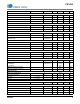
Notes: 1. Threshold is characterized as a percentage of the full-scale boost output voltage, V
BST(full)
2. The CS1680 has an internal shunt regulator that limits the voltage on the VDD pin. V
Z
, the shunt regulation voltage, is defined in
the VDD Supply Voltage section on page 4.
3. For test purposes, load capacitance C
L
is connected to gate drive pins and is equal to 0.25nF.
4. Mode1 algorithm regulates value at the trough of the rectified waveform.
5. Mode2 algorithm regulates boost output voltage at the phase cut of each rectified waveform.
6. LED output current begins changing if boost output voltage is outside the Mode3 algorithm regulation range.
7. Accelerated increase in LED output current begins at clamp on and continues until the boost output voltage falls to clamp off.
8. External circuitry should be designed to ensure that the ZCD current drawn from the internal clamp diode when it is forward biased
does not exceed specification.
9. The conductance is specified in Siemens (S or 1/). Each LSB of the internal ADC corresponds to 250nS or one parallel 4M
resistor. Full scale corresponds to 256 parallel 4M resistors or 15.625k.
10. Specifications are guaranteed by design and are characterized and correlated using statistical process methods.
3.2 Thermal Resistance
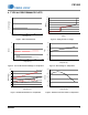
3.3 Absolute Maximum Ratings
Characteristics conditions:
All voltages are measured with respect to GND.
Note: 11. Transient current of up to 170mA will not cause SCR latch-up
12. Long-term operation at the maximum junction temperature will result in reduced product life. Derate internal power dissipation at
the rate of 50 mW /°C for variation over temperature.
WARNING:
Operation at or beyond these limits may result in permanent damage to the device.
Normal operation is not guaranteed at these extremes.
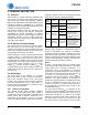
Internal Overtemperature Protection (iOTP)
Thermal Shutdown Threshold
(Note 10) T
SD
- 135 - ºC
Thermal Shutdown Hysteresis
(Note 10) T
SD(Hy)
-14-ºC
Symbol Parameter TSSOP Unit
JA
Junction-to-Ambient Thermal Impedance 2 Layer PCB
4 Layer PCB
138
103
°C/W
°C/W
JC
Junction-to-Case Thermal Impedance 2 Layer PCB
4 Layer PCB
44
28
°C/W
°C/W
Pin Symbol Parameter Value Unit
6V
DD
IC Supply Voltage 18.5 V
1, 2, 3, 8, 9,
10, 13, 14, 15, 16
Analog Input Maximum Voltage -0.5 to (V
DD
+0.5) V
1, 2, 3, 8, 9,
10, 13, 14, 15, 16
Analog Input Maximum Current
(Note 11) 5mA
5, 11, 12 V
GD
Gate Drive Output Voltage -0.3 to (V
DD
+0.3) V
5, 11, 12 I
GD
Gate Drive Output Current -1.0 / +0.5 A
-P
D
Total Power Dissipation 100 mW
-T
J
Junction Temperature Operating Range (Note 12) -40 to +125 °C
-T
Stg
Storage Temperature Range -65 to +150 °C
All Pins ESD
Electrostatic Discharge Capability Human Body Model
Charged Device Model
2000
500
V
V
Parameter Condition Symbol Min Typ Max Unit