
User guide
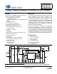


CS1615A/16A
6 DS1033PP2
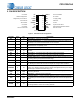
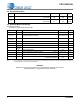
3.2 Thermal Resistance
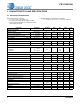
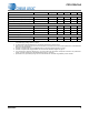
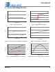
3.3 Absolute Maximum Ratings
Characteristics conditions:
All voltages are measured with respect to GND.
Note: 8. Long-term operation at the maximum junction temperature will result in reduced product life. Derate internal power dissipation at
the rate of 50 mW /°C for variation over temperature.
WARNING:
Operation at or beyond these limits may result in permanent damage to the device.
Normal operation is not guaranteed at these extremes.
Symbol Parameter SOIC TSSOP Unit
JA
Junction-to-Ambient Thermal Impedance 2 Layer PCB
4 Layer PCB
119
105
138
103
°C/W
°C/W
JC
Junction-to-Case Thermal Impedance 2 Layer PCB
4 Layer PCB
50
44
44
28
°C/W
°C/W
Pin Symbol Parameter Value Unit
14 V
DD
IC Supply Voltage 18.5 V
1,2,8,9,
10,11,16
Analog Input Maximum Voltage -0.5 to (V
DD
+0.5) V
1,2,8,9,
10,11,16
Analog Input Maximum Current 5 mA
13 V
GD
Gate Drive Output Voltage -0.3 to (V
DD
+0.3) V
13 I
GD
Gate Drive Output Current -1.0 / +0.5 A
5I
SOURCE
Current into Pin 1.1 A
3I
CLAMP
Clamp Output Current 15 mA
-P
D
Total Power Dissipation 400 mW
-T
J
Junction Temperature Operating Range (Note 8) -40 to +125 °C
-T
Stg
Storage Temperature Range -65 to +150 °C
All Pins ESD
Electrostatic Discharge Capability Human Body Model
Charged Device Model
2000
500
V
V