
User guide

CS1610/11/12/13
DS929F6 3
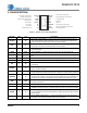
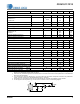
2. PIN DESCRIPTION
Pin Name
Pin # I/O
Description
BSTAUX
1IN
Boost Zero-current Detect — Boost inductor demagnetization sensing input for
zero-current detection (ZCD) information. The pin is connected to the PFC boost
inductor auxiliary winding through an external resistor divider.
IAC
2IN
Rectifier Voltage Sense — A current proportional to the rectified line voltage is fed
into this pin. The current is measured with an A/D converter.
CLAMP
3OUT
Voltage Clamp Current Source — Connect to a voltage clamp circuit on the output
of the boost stage.
SGND
4PWR
Source Ground — Common reference current return for the SOURCE pin.
SOURCE
5IN
Source Switch — Connected to the source of the boost stage external high-voltage
FET.
NC
6IN
No Connect — Connect this pin to VDD using a pull-up resistor.
NC
7IN
No Connect — Connect this pin to VDD using a pull-up resistor.
IPK
8IN
Boost Peak Current — Connect a resistor to this pin to set the peak current of the
boost circuit.
FBGAIN
9IN
Second Stage Gain — Connect a resistor to this pin to set the switching frequency
gain for the second stage.
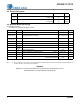
eOTP
10 IN
External Overtemperature Protection — Connect an external NTC thermistor to
this pin, allowing the internal A/D converter to sample the change to NTC resistance.
FBSENSE
11 IN
Second Stage Current Sense — The current flowing in the second stage FET is
sensed across a resistor. The resulting voltage is applied to this pin and digitized for
use by the second stage computational logic to determine the FET's duty cycle.
GND
12 PWR
Ground — Common reference. Current return for both the input signal portion of the
IC and the gate driver.
GD
13 OUT
Gate Driver — Gate drive for the second stage power FET.
VDD
14 PWR
IC Supply Voltage —
Connect a storage capacitor to this pin to serve as a reservoir for
operating current for the device, including the gate drive current to the power transistor
.
FBAUX
15 IN
Second Stage Zero-current Detect — Second stage inductor sensing input. The
pin is connected to the second stage inductor’s auxiliary winding through an external
resistor divider.
BSTOUT
16 IN
Boost Output Voltage Sense — A current proportional to the boost output is fed
into this pin. The current is measured with an A/D converter.
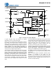
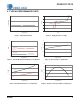
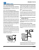
No Connect
Source Switch
Source Ground
Boost Zero-current Detect
Rectifier Voltage Sense
Boost Peak Current
NC
NCNo Connect
SOURCE
SGND
BSTAUX
eOTP External Overtemperature Protection
FBSENSE Second Stage Current Sense
GND Ground
GD Gate Driver
VDD
IC Supply Voltage
FBAUX
Second Stage Zero-current Detect
BSTOUT
Boost Output Voltage Sense
IAC
CLAMP
Voltage Clamp Current Source
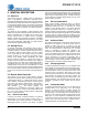
16-lead SOICN
IPK
FBGAIN Second Stage Gain
7
6
5
4
3
2
1
10
11
12
13
14
15
16
8
9
Figure 2. CS1610/11/12/13 Pin Assignments