
Manual

AN346
3
2. PCB LAYOUT
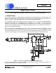
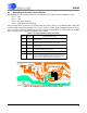
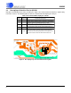
Figure 1 and Figure 2 show a schematic and layout for a 90W PFC stage. The board is a single-layer PCB
with through-hole components on the top side, surface-mount components & signal routing on the bottom.
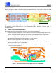
Figure 2. Single-layer PCB Layout for a 120W PFC-only Application Using the CS1500
The following sections demonstrate the best layout practices when designing a system using the
CS1500/CS1501.
2.1 Power Layout Recommendations
The following are good layout guidelines for a PFC stage or fluorescent ballast.
– Keep the main power components such as inductor, FET, diode, and output bulk capacitor as close
together as possible. Minimize trace impedance by keeping connections as short & wide as
possible. Fast power switching currents generate noise in proportion to the trace impedance.
– The power-stage ground and the signal ground must be separated.
– Input decoupling capacitors should be placed close to the inductor.
– EMI filter should be placed as close to AC inlet as possible.
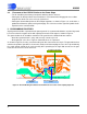
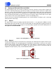
– The MOSFET gate drive loop length should be minimized, as shown in Figure 3. This applies to
both the positive (drive) path & return (GND).
– Current sense resistor return (GND) should be close to the output bulk capacitor negative (GND)
to reduce interference with the IC.
Figure 3. Gate-to-Ground Current Paths Between CS1501 and MOSFET
EMI Filter Boost PFC Section
Low Voltage IC Section