
User Manual


CS1501
6 DS927F4
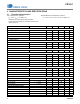
3.2 Absolute Maximum Ratings
Characteristics conditions:
All voltages are measured with respect to GND.
Notes: 5. Long-term operation at the maximum junction temperature will result in reduced product life. Derate internal power
dissipation at the rate of 50mW/ °C for variation over temperature.
WARNING:
Operation at or beyond these limits may result in permanent damage to the device.
Normal operation is not guaranteed at these extremes.
Pin Symbol Parameter Value Unit
8V
DD
IC Supply Voltage 19 V
1,2.3,4,5 - Analog Input Maximum Voltage -0.5 to (V
DD
+0.5) V
1,2,3,4,5 - Analog Input Maximum Current 50 mA
7V
GD
Gate Drive Output Voltage -0.3 to (V
DD
+0.3) V
7I
GD
Gate Drive Output Current -1.0 / +0.5 A
-P
D
Total Power Dissipation @ T
A
=50°C 600 mW
-
JA
Junction-to-Ambient Thermal Impedance 107 °C/W
-T
A
Operating Ambient Temperature Range -40 to +125 °C
-T
J
Junction Temperature Operating Range
5
-40 to +125 °C
-T
Stg
Storage Temperature Range -65 to +150 °C
All Pins ESD
Electrostatic Discharge Capability Human Body Model
Charged Device Model
2000
500
V
V