
User Manual


CS1501
DS927F4 3
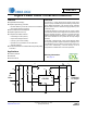
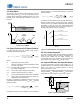
2. PIN DESCRIPTION
CSPFC Current Sense
IFBLink V oltage Sense
ZCD PFC Zero-current Detect
GND
Ground
GD P FC Gate D r iv er
VDD IC Supply Voltage
STBYStandby
IA CRectifier Voltage Sense
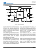
4
3
2
1
5
6
7
8
8-lead SOIC
Figure 2. CS1501 Pin Assignments
Pin Name
Pin # I/O
Description
IFB
1IN
Link Voltage Sense — A current proportional to the output link voltage of the PFC is
input here. The current is measured with an ADC.
STBY
2IN
Standby — A voltage below 0.8V puts the IC into a non-operating, low-power state.
The input has an internal 600k pull-up resistor to the V
DD
pin.
IAC
3IN
Rectifier Voltage Sense — A current proportional to the rectified line voltage is input
here. The current is measured with an ADC.
CS
4IN
PFC Current Sense — The current flowing in the PFC MOSFET is sensed through a
resistor. The resulting voltage is applied to this pin and digitized for use by the PFC
computational logic to limit the maximum current through the power FET.
ZCD
5IN
PFC Zero-current Detect — Boost Inductor demagnetization sensing input for
zero-current detection (ZCD) information. The pin is externally connected to the PFC
boost inductor auxiliary winding through an external resistor divider.
GND
6PWR
Ground — Common reference. Current return for both the input signal portion of the IC
and the gate driver.
GD
7OUT
PFC Gate Driver — The totem pole stage is able to drive the power MOSFET with a
peak current of 0.5A source and 1.0A sink.
V
DD
8PWR
IC Supply Voltage — Supply voltage of both the input signal portion of the IC and the
gate driver. A storage capacitor is connected on this pin to serve as a reservoir for oper-
ating current for the device, including the gate drive current to the power transistor. This
pin is clamped to a maximum voltage (V
z
) by an internal zener function.