CS48L10 32-Bit Audio DSP Product CRD48L10-4in4out Board Manual Copyright Cirrus Logic, Inc. 2012 (All Rights Reserved) http://www.cirrus.
CS48L10 Contacting Cirrus Logic Support For all product questions and inquiries, contact a Cirrus Logic Sales Representative. To find the one nearest you, go to www.cirrus.com. IMPORTANT NOTICE Cirrus Logic, Inc. and its subsidiaries (“Cirrus”) believe that the information contained in this document is accurate and reliable. However, the information is subject to change without notice and is provided “AS IS” without warranty of any kind (express or implied).
CS48L10 Chapter 1 Introduction to the CRD48L10-4in4out Board 1.1 Requirements ..................................................................................................................................................... 1-1 1.2 CRD48L10-4in4out Main Board Description ...................................................................................................... 1-1 1.3 Introduction to the CRD48L10 Kit ............................................................................................
CS48L10 4.2 Powering Board .................................................................................................................................................. 4-1 4.3 Monitoring Audio ................................................................................................................................................. 4-2 4.4 Selecting Audio Input Source .............................................................................................................................
1.1 Requirements Chapter 1 Introduction to the CRD48L10-4in4out Board Table 1-1. CRD48L10 Kit Contents Item Quantity Cirrus Logic CRD48L10 Board 1 Cirrus Logic CRD48L10 MCU USER INTERFACE Board 1 Cirrus Logic CDB-MCU-DEBUG Board 1 USB cable A-Mini 2 Stereo audio cables RCA female, 3.5 mm male 1 5x2 ribbon cable 1 7x2 ribbon cable 1 15x2 ribbon cable 1 TOSLINK female to TOSLINK mini male adapter 2 Doc card universal DSP 1 Doc evaluation board disclaimer notice 1 1.
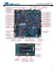
1.3 Introduction to the CRD48L10 Kit CRD48L10 – 4IN4OUT +5V -> +3v3 (SPDIF) Coax RX Mini OPTICAL RX RMCK CLOCKS CS8416 CS8406 +3v3 CLK HDR 12.288 MHz OSC Control & MP3 I2S DAI2 I2S DAO2 I2S Clocks CHAS CS48L10 DSP +1v0 / +1v2 +1v8 I2S DAI1 I2S DAO1 SPKR-R EAR Level Translation SCP Probe HDR (SPI, I2C) I/O Expander I2S Probe HDR (DAI[2:1], DAO[2:1], Clocks) MIC1 +1v8 +5v0 MIC2 uHDMI c INPUT SOURCE DISPLAY +4v0 -> +3.
1.3 Introduction to the CRD48L10 Kit Figure 1-2. CRD48L10-4in4out Figure 1-3.
1.3 Introduction to the CRD48L10 Kit Figure 1-4. CDB-MCU-DEBUG Board Figure 1-5.
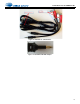
1.3 Introduction to the CRD48L10 Kit Figure 1-6. USB and 1/8” to RCA Cables Figure 1-7.
2.1 Audio Inputs Chapter 2 Input/Output Specifications 2.1 Audio Inputs 2.1.1 Analog Line Input • Connector Type: 1/8 inch (3.5mm) stereo Female • Absolute Maximum Signal Level: +2.1 V • Absolute Minimum Signal Level: –0.3 V • Full Scale Amplitude (PGA VOL = 0 dB): 1.44 Vpp • Reference Designators: J2 (LINE IN) 2.1.2 Analog Microphone Input • Connector Type: 1/8 inch (3.5mm) stereo Female • Absolute Maximum Signal Level: +2.1 V • Absolute Minimum Signal Level: –0.
2.2 Audio Outputs 2.2 Audio Outputs 2.2.1 Connector Type: 1/8 inch (3.5mm) stereo Female • Full Scale Output: 2.9 Vpp • Reference Designators: J3 (LINE OUT) 2.2.2 Headphone Output • Connector Type: 1/8 inch (3.5mm) stereo Female • Full Scale Output: 1.5 Vpp • Power: 2 x 17 mW (at THD+N = –60 dB) • Minimum Load: 16 ohms • Reference Designator: J5 (HEADPHONE) Note: 2.2.3 This output has the same data as J3 (LINE OUT).
2.3 Digital Control Probe Points 2.3 Digital Control Probe Points 2.3.1 DSP Control • Connector Type: 100-MIL Male Header (5x2) • Absolute Maximum Input Signal Level: +6.5 V • Absolute Minimum Input Signal Level: –0.5 V • Maximum Signal Output Level: +V_PROBE • Reference Designators: JP3 (CTRL HDR), TP15 2.3.2 DSP Debug • Connector Type: 100-MIL Male Header (4x1) • Absolute Maximum Input Signal Level: +2.0 V • Absolute Minimum Input Signal Level: –0.
2.4 DSP Composer Control Header 2.3.7 • Main Clock Connector Type: 100-MIL Male Header (2x1) • Absolute Maximum Input Signal Level: +6.0 V • Absolute Minimum Input Signal Level: –0.5 V • Reference Designators: TP4 (CLKIN) 2.4 DSP Composer Control Header • Connector Type: 50-MIL Male Header (15x2) • Absolute Maximum Input Signal Level: +2.0 V • Absolute Minimum Input Signal Level: –0.5 V • Maximum Signal Output Level: +1.8 V • Reference Designators: JP2 2.
2.9 MCU DEBUG C-2 Programming Header 2.9 MCU DEBUG C-2 Programming Header This header is used to program the MCU from a CDB-MCU-DEBUG dongle (P4/C2-OUT connector) OR the Silicon Labs programming dongle. • Connector Type: Shrouded 100-MIL Male Header (5x2) • Absolute Maximum Input Signal Level: +3.6 V • Absolute Minimum Input Signal Level: –0.5 V • Maximum Signal Output Level: +1.8 V • Reference Designators: JP4 2.
3.1 S1 Button Control (No LCD) Chapter 3 Standalone Modes The CRD48L10-4in4out has multiple audio input and output ports. All available data flow paths are shown in the diagram in Fig. 3-1.
3.1 S1 Button Control (No LCD) Figure 3-2. CRD48L10-4in4out S1 Control Only 3.1.2 Selecting Input Audio Source Input selection is controlled with the S1 button, as shown in Fig 3-3, on the CRD48L10 board. By default, the Input will DSP play back an MP3 from on-board FLASH U9. There is an LED next to each input to indicate which input is active, except when in FLASH playback where no input LED will be illuminated. Figure 3-3.
3.1 S1 Button Control (No LCD) The MCU will cycle through the inputs when the button S1 is pressed from FLASH > LINE IN > MIC 1 & 2 > S/PDIF > FLASH. LED locations are shown in Fig. 3-4 to Fig. 3-6. If the MCU-USER-INTERFACE board is attached, the LCD also displays the active input. Figure 3-4. LINE IN Active Figure 3-5.
3.1 S1 Button Control (No LCD) Figure 3-6. S/PDIF OPTICAL Active Each of the input modes is described in the following sections. The MCU configures the data paths shown feeding the DSP in the following data path diagrams. Inactive paths are shown in gray. The DSP project determines how the audio is processed and which audio goes out each DAO port. The default DSP projects programmed into the CRD48L10 are configured to process the audio paths shown in blue. 3.1.
3.1 S1 Button Control (No LCD) SCLK (ASP/XSP) LRCLK (ASP/XSP) SCLK LRCLK MCLK (CS42L73) (CS48L10) MCLK1 CLOCK OSCILLATOR 12.288 MHz Figure 3-8. Clocking for FLASH Playback–DSP Master This is the default configuration after power up of the CRD48L10-4in4out. Power up and connect headphones to the HEADPHONE jack or a speaker to the LINE OUT jack, and you will hear audio playing in a continuous loop. 3.1.
3.1 S1 Button Control (No LCD) The S/PDIF receiver is configured to automatically switch between the on-board oscillator and the clock recovered from an incoming S/PDIF stream. In the previous diagram, any time a valid S/PDIF stream is presented to the CS8416, the system audio clock will be locked to the Fs of the incoming stream. The S/PDIF cable should be removed when the on-board oscillator (or TP4) is meant to master audio clocks. 3.1.
3.2 MCU UI Controlled 3.1.6 S/PDIF Digital MIC VSP IN VSP OUT Headphone Outputs (CS42L73) MIC1 DAC Line Outputs (L&R) MIC2 ASP OUT ADC DAI1 DAO 1 ASP IN Speakerphone (L) (CS48L10) Line In (L) XSP OUT Line In (R) DAI2 DAO2 XSP IN DAC SPDIF RX (CS8416) Level Translation AMP (CS3501 ) Speakerphone (R) EAR SCP Mini Optical RX Or 1/8" Coax (L&R) Level Translation SPDIF TX (CS8406 ) Mini Optical TX Figure 3-13.
3.2 MCU UI Controlled Figure 3-15. CRD48L10-4in4out MCU UI Control 1. The LCD will then display the current revision of the on board C8051F930 MCU, as shown below: 2. The MCU will attempt to read a micro_condenser image from the SPI FLASH. If it fails you will get the following error: 3. The MCU will cycle through displays showing the status of the Audio Source, Project:, and Snapshot: 4.
3.2 MCU UI Controlled There are four projects available in the default MCU code shipped with the CRD48L10: • MP3 Decode from FLASH • LINE IN • MIC IN • S/PDIF IN Each project is described in the following sections. 3.2.2.1 MP3 Decode from FLASH (U9) Project This project is selected, as shown in Fig. 3-17. Figure 3-17. MP3 Decode from FLASH This project is the same as described in Section 3.1.3. There is only one snapshot available for this project. 3.2.2.
3.2 MCU UI Controlled Digital MIC VSP IN VSP OUT Headphone Outputs (CS42L73) MIC1 DAC MIC2 ASP OUT ADC DAI1 DAO1 ASP IN Speakerphone (L) (CS48L10) Line In (L) XSP OUT Line In (R) DAO2 DAI2 XSP IN DAC AMP (CS3501 ) SPDIF RX (CS8416) Level Translation Speakerphone (R) EAR SCP Mini Optical RX Or 1/8" Coax (L&R) Line Outputs (L&R) Level Translation SPDIF TX (CS8406 ) Mini Optical TX Figure 3-21.
3.2 MCU UI Controlled SCLK SCLK (ASP/XSP) LRCLK LRCLK (ASP/XSP) Level Translation SCLK LRCLK (CS42L73) MCLK SPDIF RX (CS8416 ) (CS48L10) Mini Optical RX Or 1/8" Coax CLOCK MCLK1 OSCILLATOR 12.288 MHz Figure 3-24. Clocking for All S/PDIF Snapshots–DSP MCLK Slave 3.2.3 Snapshot Menu A project defines the firmware modules downloaded to the DSP, and the data routing on the board. A snapshot is simply a reconfiguration of the DSP using the same firmware and data routing.
3.2 MCU UI Controlled The following are menu choices under Clock Source: • Default 12.288 MHz oscillator • CLK IN header TP4 3.2.6 • TP4 supports voltages from +1.8 V to +5 V. • A shunt must be installed on TP30 only when using TP4. I2C Control Source Menu An I2C bus is used to configure the CS42L73 codec, S/PDIF Rx, and S/PDIF Tx. By default, the MCU configures all components on the board for data flow selected.
4.1 Jumper Settings Chapter 4 Quick Start for the CRD48L10-4in4out The easiest use case of the CRD48L10-4in4out requires power (via the mini-USB connector) and some method of listening to audio. The CRD48L10 is configured for USB power from a PC in Fig. 4-1, and the audio can be monitored using headphones. Figure 4-1.
4.3 Monitoring Audio 4.3 Monitoring Audio By default, all audio outputs of the CRD48L10 are active. Any of the outputs listed in Section 2.2 can be connected to a speaker or headphones with compatible impedance characteristics. 4.4 Selecting Audio Input Source The S1 button or rotary encoder knob can be used to select an audio source. Input options are described in Section 3.1. 4.5 USB Control of CRD48L10-4in4out The USB1 connector does not provide USB control of the CRD48L10-4in4out.
Chapter 5 Using DSP Composer™ with CRD48L10-4in4out The CRD48L10-4in4out can be controlled using the DSP Composer™ application through the CDB-MCU-DEBUG board. A detailed description of how to connect to the PC and configure the CDB-MCU-DEBUG for use with DSP Composer can be found in the CDB-MCU-DEBUG Controller User's Manual. The CDB-MCU-DEBUG must be connected to JP2 as shown in Fig. 5-1. Figure 5-1. CDB-MCU-DEBUG Connected to JP2 of CRD48L10-4in4out The CRD48L10-4in4out has three .
Figure 5-3. S/PDIF Pass-thru • An S/PDIF + LINE-IN project is shown in Fig. 5-4. Figure 5-4.
6.1 Checking the Revision of MCU Code in the Board Chapter 6 Updating the MCU Image The CRD48L10 MCU is not automatically updated to the latest version. The user must compare the revision of the MCU code on the board to the revision that is included in the SDK and manually perform the update. 6.1 Checking the Revision of MCU Code in the Board When powering on the CRD48L10 board, the MCU displays the revision of its code for three seconds. The user must have the MCU-USER-INTERFACE connected.
6.3 Programming the MCU Figure 6-3. Programming Successful Power cycle the CRD48L10-4in4out board, and then the LCD will indicate the new revision of MCU code, as shown in Fig. 6-4. Figure 6-4.
7.1 Generate Deliverables Chapter 7 Using Micro-Condenser to Create and Load a FLASH Image This section describes how to create a standalone binary image using micro-condenser that can be loaded into the CRD48L10. Different projects and snapshots can be chosen using the buttons, rotary switch, and LCD on the board in standalone mode using DSP Composer. 7.1 Generate Deliverables Use the following process to generate deliverables: 1. Open the desired .
Chapter 8 Programming MP3 FLASH 1. Configure CRD48L10 as described in CDB-MCU-DEBUG Controller User’s Manual, and launch a command console window. 2. Within command console, CD to the CS48Lxx\apps\crd48l10-4in-4out\ board directory. 3. Run the script “program_spi_flashA.bat ” where is the name of the image for the FLASH. 4. When programming is complete, the console window should read “Image validated by read/compare” as shown in Fig. 8-1. Figure 8-1. Programming MP3 FLASH 5.
9.1 SPI Master Boot Chapter 9 Master Boot Usage Note: Master boot usage is only supported in SDK 6.6.x or later versions of the SDK. 9.1 SPI Master Boot 1. For any CS48L10 .cpa file, in DSP Composer, access File > Properties. 2. Set the “Board comm mode” to “Master SPI”. Figure 9-1. Board Comm Mode 3. Select the post boot comm mode by selecting the appropriate mode from the “SCP mode” dropdown menu. Figure 9-2. SCP Mode 4. Ensure that the “Use JP2 board control header” checkbox is selected. 5.
9.2 I2C Master Boot Note: Programming the Master Boot image erases the MP3 content. 9.2 I2C Master Boot I2C master boot is not supported on CRD48L10_4in4out.
10.1 External Control of CS48L10 Chapter 10 External Control of CRD48L10-4in4out External control of the CRD48L10 can be viewed as two different components: • External Control of CS48L10 DSP • External Control of CRD48L10-4in4out Audio Subsystem Some evaluations of the CS48L10 using an external controller may require only configuration of the DSP while using the built-in audio paths of the CRD48L10-4in4out. For this reason, we have split external control options into two parts.
Chapter 11 Measuring Power Current measurement points are available for the CS48L10, CS42L73, and for the entire CRD48L10 using the provided current measurement headers. Table 11-1. Power Measurement Headers Header Voltage Signal Bypass Resistor TP20 +1.0 V – +1.2 V CS48L10 Core Power Rail R170 TP21 +1.8 V CS48L10/O Power Rail R171 TP22 +4.0 V Battery Voltage for CS42L73 R180 TP23 +1.8 V CS48L73 + 1.8 V Power Rail R192 P16 +4.0 V Main Power Rail for CRD48L10-4in4out N/A Figure 11-1.
Accuracy of these measurements depends on the DMM used for performing the current/voltage measurements. DMM’s tend to have more accuracy with small values when measuring current than when measuring voltage. For that reason, when measuring standby current, it may be necessary to remove the bypass resistors and measure current directly between the pins of the headers. Table 11-2. Typical Standby Current Measurements Header Voltage Typical Current TP20 +1.0 V – +1.2 V 11 µA TP21 +1.8 V 0.8 µA TP22 +4.0 V 1.
Chapter 12 Using Analog MEMS Microphones When shipped, the CRD48L10-4in4out is configured to work with ECM microphones. The CS472L73 provides a bias voltage of +2.0 V to +2.75 V to the MIC1 and MIC2 inputs through the J8 and J9 jumpers. The exact bias voltage is configurable through the MIC_BIAS_CTRL bit within the CS42L73 registers. The AMEMS microphone provides its own bias level, so J8 and J9 need to be removed to use the AMEMS Microphone module. Figure 12-1. MIC Bias Jumpers Table 12-1.
Figure 12-3. AMEMS HDMI Board Wired to MIC Boards Figure 12-4. AMEMS Cabled to CRD48L10-4in4out The AMEMS can then be used with the standard MIC-IN project on the CRD48L10-4in4out.
Chapter 13 Interfacing to Telit GSM Module A special adapter board is available from Cirrus to connect the VSP port from the CRD48L10 to a Telit wireless module to emulate cell phone communication.
Chapter 14 Schematic, Layout, BOM The design files for the CRD48L10_4in4out are included in the crd48l10_4in_4out.exe installer. When installed in the SDK install directory, the schematic can be found in the following directory: \schematics\crd48l10_4in4out_Rev_X Because each revision of a board has its own directory, the ‘X’ in the file name above indicates the board revision that matches the revision of the board being used.
Chapter 15 Revision History Revision DB1 Date Changes November, 2012 Initial release.