
Instruction Manual


Table Of Contents
- Features
- Description
- 1. General information
- 2. Schematic Description
- 3. Grounding and Layout
- 4. References
- 4.1 ADDENDUM
- Figure 1. Block Diagram
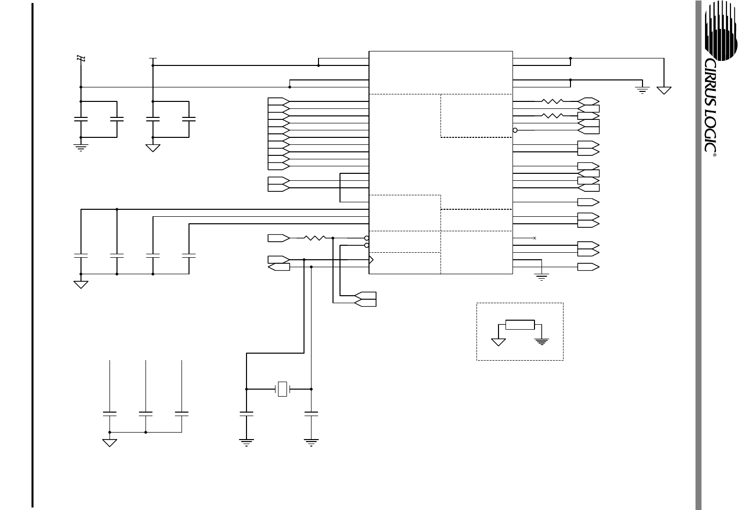
- Figure 2. CS4202 Audio Codec
- Figure 3. Analog Inputs
- Figure 4. Center Channel, Surround, and Sub-Woofer Outputs
- Figure 5. Front Channel and Headphone Sense Output
- Figure 6. S/PDIF Optical Output
- Figure 7. CNR Connector
- Figure 8. Phase Locked Loop
- Figure 9. Auto Demotion and Serial Buffers
- Figure 10. PCB Layout: Top Assembly Drawing
- Figure 11. PCB Layout: Top Layer
- Figure 12. PCB Layout: Bottom Layer
- Figure 13. PCB Layout: Drill Drawing
- Figure 14. PCB Layout: Top Silkscreen
- 4.1 ADDENDUM
- 5. bill of materials
CRD4202-1
8 DS549RD1A1
C14
22pF
NPO
C15
22pF
NPO
C3
0.1uF
Z5U
C4
0.1uF
Z5U
C1
0.1uF
Z5U
R55 0
C2
0.1uF
Z5U
R2 47
R1 47
Y1
24.576 MHz
U1 CS4202
LINE_OUT_R
36
MONO_OUT
37
AVdd2
38
HP_OUT_L
39
GPIO1/SDOUT
44
HP_OUT_R
41
AVss2
42
GPIO0/LRCLK
43
HP_OUT_C
40
GPIO4/SDO2
34
GPIO3
33
GPIO2
32
HPCFG
31
DVdd1
1
XTL_IN
2
XTL_OUT
3
DVss1
4
SDATA_OUT
5
BIT_CLK
6
DVss2
7
SDATA_IN
8
SYNC
10
DVdd2
9
RESET#
11
PC_BEEP
12
PHONE
13
AUX_L
14
AUX_R
15
VIDEO_IN_L
16
VIDEO_IN_R
17
CD_L
18
CD_C
19
CD_R
20
MIC1
21
MIC2
22
LINE_IN_L
23
LINE_IN_R
24
AVdd1
25
AVss1
26
REFFLT
27
Vrefout
28
AFLT1
29
AFLT2
30
SPDIF_OUT
48
EAPD/SCLK
47
ID1#
46
ID0#
45
LINE_OUT_L
35
C5
2.2uF
Y5V
C8
NPO
C7
1000pF
NPO
C6
0.1uF
X7R
C11
1000pF
NPO
C12
1000pF
NPO
C13
1000pF
NPO
LINE_OUT_L
LINE_OUT_R
MONO_OUT
DGND
DGNDAGND
+3.3VD
DGND
AGND
AGND
DGND
DGND
AGND
+5VA
ABITCLK
LINE_IN_R
ASYNC
ASDOUT
PRIM_DN#
ASDIN
ARST#
XTAL_IN
LINE_OUT_L
LINE_OUT_R
LINE_IN_L
XTAL_OUT
LRCLK
SPDIF_OUT
SDOUT1
HP_OUT_C
SDOUT0
HP_OUT_R
MONO_OUT
GPIO2
HP_OUT_L
SCLK
ID1#
ID0#
AUX_IN_L
MIC1
CD_IN_R
AUX_IN_R
PHONE_IN
CD_IN_L
VIDEO_IN_L
PC_BEEP
VIDEO_IN_R
CD_C
For 6 channel
configuration GPIO3 (pin 33)
is tied to
DGND.
DGND
AGND
GND TIE 0.050 inches
Figure 2. CS4202 Audio Codec