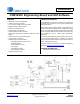
CDB5490U CDB5490U Engineering Board and GUI Software Features General Description • • • • • • • • The CDB5490U is an extensive tool designed to evaluate the functionality and performance of Cirrus Logic’s CS5490 power measurement device.
CDB5490U IMPORTANT SAFETY INSTRUCTIONS Read and follow all safety instructions prior to using this demonstration board. This Engineering Evaluation Unit or Demonstration Board must only be used for assessing IC performance in a laboratory setting. This product is not intended for any other use or incorporation into products for sale. This product must only be used by qualified technicians or professionals who are trained in the safety procedures associated with the use of demonstration boards.
CDB5490U TABLE OF CONTENTS 1. HARDWARE .............................................................................................................................................. 5 1.1 Introduction ........................................................................................................................................ 5 1.2 Evaluation Board Overview ................................................................................................................ 5 1.3 Analog Section ........
CDB5490U LIST OF FIGURES Figure 1. CDB5490U Assembly Drawing and Default Configuration................................................................ 5 Figure 2. Voltage Channel — Low-voltage Input .............................................................................................. 6 Figure 3. Voltage Channel — High-voltage Input ............................................................................................. 7 Figure 4. Current Channel — Low-voltage Input ...........................
CDB5490U 1. HARDWARE 1.1 Introduction The CDB5490U evaluation board provides a convenient means of evaluating the CS5490 energy measurement IC. The CDB5490U evaluation board operates from a single USB or 5V power supply. An optional 3.3V power supply input is available for powering the CS5490 directly. The evaluation board interfaces the CS5490 to a PC via a USB cable. To accomplish this, the board comes equipped with a C8051F342 microcontroller and a USB interface.
CDB5490U 1.3 Analog Section The analog section of the CDB5490U is highly configurable. Onboard signal conditioning options for the voltage and current channels enable most applications to interface directly to the sensors. The following two sections define the voltage and current channel configurations. 1.3.
J6 R15 422K R14 422K J4 R12 422K CDB5490U R8 422K LINE NEUTRAL CDB5490U J45 LINE VIN+ R5 1K R6 1K GND 0.027UF C4 0.027UF J11 C9 CS5490 R7 1K VIN- Figure 3. Voltage Channel — High-voltage Input The default attenuation network provides the following attenuation: 1k 1 ---------------------------------------= ------------ 4 422k + 1k 1689 With the CS5490 input range of 250mVp at maximum AC line input of: 250mVp 300Vrms = ----------------------- 1689 2 is acceptable.
CDB5490U 1.3.2 Current Sensor Connection Current input options include an external signal (via screw terminals or XLR connectors) or GND. Table 2 illustrates the options available. Table 2.
CDB5490U 1.4 Digital Section The digital section contains the microcontroller, USB interface, LCD, optical isolation, JTAG header, reset circuitry, and external interface headers (J17 and J19). The microcontroller interfaces the UART of the CS5490 with the USB connection to the PC, enabling the GUI software to access all of the CS5490 registers and functions. 1.4.1 Serial Port Selection Communication to the CS5490 is provided through a standard UART.
CDB5490U 1.4.2 Interface to Microcontroller Interface headers J17 and J19 are provided to allow the CDB5490U to be connected to an external energy registration device or an external microcontroller. Interface header J17 provides direct access to the CS5490 pins while interface header J19 provides an isolated connection. It is imperative to use the isolated connection (J19) when high-voltage signals are used. Failure to use isolation can result in damage to components or electrical shock.
CDB5490U 1.5 Power Supply Section Table 4 illustrates the power supply connections on the evaluation board. The positive analog (VDDA) for the CS5490 can be supplied using the +3.3V binding post (J36 and J37) or the onboard +3.3V regulator. Jumper J38 allows the VDDA supply to be sourced from the +3.3V binding post (J37) or the regulated +3.3V supply. The DC-DC converter (U8) powers the onboard +3.3V regulator.
CDB5490U 1.6 Typical Sensor Connections The CDB5490U evaluation board provides connections directly to several types of sensors. Flexible onboard filter networks provide a convenient configuration for three common transducers: current shunt, current transformer (CT), or Rogowski coil. 1.6.1 Shunt Power Meter Example An inexpensive current shunt configuration is easily achievable with the CDB5490U evaluation board.
CDB5490U 1.6.2 Current Transformer Power Meter Example A slightly more expensive option is to use a current transformer (CT) to connect the AC current to the CDB5490U evaluation board. Figure 7 depicts the voltage and current connections for a CT sensor and its associated filter configurations. NEVER “open circuit” a CT. Make sure that all signals are well connected before the power source is turned on. Extreme care should be taken when connecting high-voltage signals to the CDB5490U evaluation board.
CDB5490U 1.6.3 Rogowski Coil Power Meter Example CDB5490U PHASE J46 R51 0 J8 J1 GND R2 100 NO POP R13 IIN+ J54 NO POP R11 IINGND J53 J7 NO POP R9 100 R1 R50 1K 0.033UF 0.033UF C6 C35 0.033UF 0.033UF C5 C34 R49 1K J6 R15 422K R14 422K R12 422K J4 R8 422K J44 J45 LINE IIN- VIN+ R5 1K R6 1K GND IIN+ CS5490 NEUTRAL Rogowski coil power meter can be easily connected to the CDB5490U evaluation board.
CDB5490U 1.7 Standalone Meter Application The CDB5490U evaluation board provides a standalone power meter using the CS5490, MCU, and LCD. The user can enable the power meter by connecting the sensors to the analog inputs, providing power to the board, and resetting the MCU by pressing the RESET switch. Refer to “Typical Sensor Connections” on page 12 for details on the sensor connections and “Power Supply Section” on page 11 for details on supply options.
CDB5490U 2. SOFTWARE The evaluation board comes with software and a USB cable to link the evaluation board to the PC. The evaluation software was developed with LabWindows®/CVI®, a software development package from National Instruments. The evaluation software is designed to run with Windows XP™ and Windows 7™. The following procedure is based on Windows XP. 2.1 Installation Procedure Follow the steps below to install the GUI: 1. Access the following web site: http://www.cirrus.com/en/support. 2.
CDB5490U 2.3 Start-up Window When the software is launched, the Start-Up Window is displayed. This window contains information about the software, including its title, revision number, and copyright date. The Start-Up Window is displayed (see Figure 10). Figure 10. GUI Start-up Window At the top of the window, a menu bar with menu items is displayed. The menu bar has four menu items: System, Cirrus Test, Connect, and Quit. Initially, System and Cirrus Test are disabled.
CDB5490U 2.4 Connect Menu The Connect menu allows the user to establish a USB communication link with CDB5490U board. After selecting the USB connect command, a popup will prompt to reset the CRD5490. The user must wait a few seconds after resetting the CRD5490 and before selecting OK on the popup. After the USB communication has been established, the CS5490 serial port is functional, as shown in Figure 12. Figure 11. Connect Menu Showing Successful USB Connection 2.4.
CDB5490U Verify that the USB cable is connected properly and that the power supply is on and connected properly to the CDB5490U. Reset the board (press the RESET button on the board) and try to set up the USB connection again. After the serial port has been selected, the MCU will read the chip ID from the CS5490. The chip revision number will be displayed in the Device field in the Start-Up Window.
CDB5490U 2.5.1 Setup Window The evaluation software provides access to the common CS5490's internal registers through the Setup Window (see Figure 16). The user can enter the Setup Window by selecting the Setup CS5490 item from the System menu. Figure 16. Setup Window In the Setup Window, all of the common CS5490 registers are displayed in hexadecimal notation and are decoded. Refer to the CS5490 data sheet for information on register functionality and definitions.
CDB5490U 2.5.1.1 Refresh Screen Button The Refresh Screen button will update the contents of the screen by reading all the register values from the CS5490. It is a good idea to press the Refresh Screen button when entering the Setup window, or after modifying any registers, to reflect the current status of the CS5490. 2.5.1.2 Reset DUT Button The Reset DUT button will software-reset the CS5490. The CS5490 will perform a software-reset, as discussed in the CS5490 data sheet.
CDB5490U 2.5.1.8 Phase Compensation The Phase Comp Register section is used to make changes to and display the contents of the CS5490's PC (Phase Compensation Control) register. The PC register allows coarse- and fine-phase adjustment on each channel of the CS5490 data path. Refer to the CS5490 data sheet for descriptions of the PC register bits. 2.5.1.9 Integrator Gain, System Gain The Integrator Gain and System Gain sections display the signal path gain in both hexadecimal and decimal format.
CDB5490U 2.5.1.16 V Sag, V Swell, and I Overcurrent Registers The registers for voltage sag, voltage swell, and overcurrent are displayed in the V Sag, V Swell, and I Overcurrent Register sections. These sections display the level and duration values of the corresponding registers in both hexadecimal and decimal format. Each register can be modified by typing a value in the corresponding decimal or HEX field. Refer to the CS5490 data sheet for detailed descriptions of these registers. 2.5.1.
CDB5490U The Refresh Screen button will update the contents of the screen by reading all the register values from the part. It is recommended to click the Refresh Screen button when entering the Calibration Window, or after modifying any registers to reflect the current status of the CS5490. 2.6.1 Save Cal and Load Cal Buttons Clicking the Save Cal button will save the calibration widow's configuration to a .txt file.
CDB5490U 2.7 Conversion Window The Conversion Window can be accessed from the System menu pull-down, Conversion menu item. The Conversion option requires the CS5490 device to be configured for 2400 or greater baud rate from the Setup Window (see Figure 18). Figure 18. Setup Window with 510638 Baud Rate When the UART is configured for a baud rate of less than 2400, the resulting error message is displayed (see Figure 19.) Figure 19.
CDB5490U status register (Status0, 1, 2) are also displayed. The Conversion Window also provides the total active, apparent and reactive power register results. Figure 20. Conversion Window 2.7.1 Single Conversion Button Pressing the Single Conversion button will cause a single conversion to be performed. After a single conversion is complete, the Result column will be updated with the values present in each data register. 2.7.
CDB5490U 2.7.5 Line Frequency Result When the AFC bit in the Config2 register is set, the Epsilon register will be calculated automatically by the CS5490 and the Line Frequency fields will be updated automatically in continuous conversion mode. If the AFC bit in the Config2 register is not set and the line frequency is other than the default value (50Hz), the line frequency must be set manually here to make Epsilon the ratio of line frequency to the output word rate (OWR).
CDB5490U 2.8.1 Data Collection Window The Data Collection Window allows the user to collect sample sets of data from the CS5490 and analyze them using time domain, FFT, and histogram plots. The Data Collection window can be accessed by pulling down the CirrusTest menu, and selecting the ADC Data Collection item (see Figure 22). Figure 22. Data Collection Window The Data Collection Window can only be accessed when the UART is operating at 510638 baud.
CDB5490U 2.8.1.4 Output Button The Output button will bring up a window in which the user can output the data to a file for later use, print out a plot, or print out the entire screen. When saving data, only the data channel being displayed on the plot will be saved to a file. 2.8.1.5 Zoom Button The Zoom button allows the user to zoom in on the plot by selecting two points in the plot area. Press the Restore button to return to the normal data plot, or press the Zoom button again to zoom in farther. 2.
CDB5490U 2.8.1.8 Configuration Window The Configuration window allows the user to set up the data collection and analysis parameters (see Figure 25). Figure 25. Data Collection Configuration Window 2.8.1.8.1 Number of Samples The Number of Samples field allows the user to select the number of samples to collect, between 16 and 524288. 2.8.1.8.2 Average When performing FFT analyses, the Average field determines the number of FFTs to average.
CDB5490U 2.8.1.8.7 Accept Button When the Accept button is pressed, the current settings will be saved and the user will return to the Data Collection window. 2.8.1.9 Collecting Data Sets To collect a sample data set: 1. In the Data Collection window, press the Config button to bring up the Configuration window and view the current settings. 2. Select the appropriate settings from the available options (see “Configuration Window” on page 30) and press the Accept button. 3.
CDB5490U 2.8.1.11 Histogram Information The following is a description of the indicators associated with histogram analysis. Histograms can be plotted in the Data Collection Window by setting the analysis type pull-down menu to Histogram (see Figure 26). The histogram plot information includes: • BIN: Displays the x-axis value of the cursor on the histogram. • MAGNITUDE: Displays the y-axis value of the cursor on the histogram. • MEAN: Indicates the mean of the data sample set.
CDB5490U 2.8.1.12 Frequency Domain Information The following describe the indicators associated with FFT (Fast-Fourier Transform) analysis. FFT data can be plotted in the Data Collection window by setting the analysis type selector to FFT (see Figure 27). The FFT information includes: • • • • • • • FREQUENCY: Displays the x-axis value of the cursor on the FFT display. MAGNITUDE: Displays the y-axis value of the cursor on the FFT display. S/PN: Indicates the signal-to-peak noise ratio (decibels).
CDB5490U 2.8.1.13 Time Domain Information The following controls and indicators are associated with time domain analysis. Time Domain data can be plotted in the Data Collection window by setting the analysis type selector to Time Domain (see Figure 28). The Time Domain plot includes: • • • • COUNT: Displays current x-position of the cursor on the time domain display. MAGNITUDE: Displays current y-position of the cursor on the time domain display.
CDB5490U 2.8.2 Data Collection to File Window The Data Collection to File window allows the user to collect instantaneous voltage and current register data over an extended period of time to a data file (see Figure 29). The Data Collection to File option requires the CS5490 device to be configured at the maximum baud rate set from the within the Setup Window (see Figure 18). The following steps are necessary for data collection to a file: 1. Provide the Time to Collect in seconds. 2.
CDB5490U 2.8.3 Setup and Test Window The Setup and Test window allows the user a way to access CS5490 registers and send commands to the CS5490 directly (see Figure 30). Figure 30. Setup and Test Window There are three types of transactions: Write register, Read register, and Send command. The CS5490 memory is organized by pages. In order to properly write a register, it is necessary to set the Page, Address, and Value to Write field and then press the WRITE button.
DS923DB5 APPENDIX A. BILL OF MATERIALS CIRRUS LOGIC CDB5490U_REV_B.bom BILL OF MATERIAL Item 1 2 3 4 5 6 7 8 9 10 11 12 13 14 15 16 17 Cirrus P/N 001-02194-Z1 001-10064-Z1 001-04187-Z1 001-10233-Z1 001-04345-Z1 001-02194-Z1 001-04523-Z1 001-01994-Z1 001-02194-Z1 001-10226-Z1 001-02189-Z1 012-00010-Z1 001-10127-Z1 012-00013-Z1 070-00055-Z1 165-00004-Z2 110-00055-Z1 Rev A A A A A A A A A A A A A A A A A Description CAP 0.1uF ±10% 25V X7R NPb 0603 CAP 15pF ±5% 50V C0G NPb 0603 CAP 0.
CIRRUS LOGIC CDB5490U_REV_B.
ECO# REV DESCRIPTION 4 1 2 NO POP 3 J32 NO POP J7 NEUTRIK R9 1K 4 GND IINIIN+ 3 R11 2.2 2 NO POP R13 1K R51 0 1 GND GND 1 IIN- 3 NO POP 2 4 J8 IIN+ 1 GND 3 NO POP 2 4 1 J30 Alan ZHA 09/24/10 ECO813 B ADDED VREG, U2, AND CHGD DC CONV., U8. A. GARZA 1/11/11 Alan ZHA 1/11/11 ECO832 B1 CIRRUS DEVICE REVISION CS5490-ISZ/A0 TO A1 ECO853 C CHGD Z3 TO CTES033V3-G, CHGD DANGER LABEL DARREN B. 2/17/11 A.
ECO# REV DESCRIPTION INC BY/DATE CHK BY/DATE USED ON EE5490U ONLY 16 15 14 13 12 11 10 9 C1 0.10uF X7R NO POP +3.3V_1 C2 0.10uF X7R NO POP NO POP-SOCKET FOR CS5490-SOIC16 C7 R30 5.1K X7R 0.10uF NO POP VDDA VDDA R31 5.1K 2 XIN_EXT GND 4 C13 X7R 0.01UF 130 R55 RESET J23 R33 10K C12 1UF C3 XIN_EXT CRYSTAL COG 15pF 1 2 3 4 5 6 7 8 X7R IINIIN+ VIN+ VIN- U1 CS5490-ISZ 0.
REV DESCRIPTION +5V_EXT +5V +3.3V_1 LCD 1 GND1 GND1 GND S1 1 5 GND1 3 RESET R45 C27 X7R 0.1uF 1K JTAG/C2 GND1 C28 X7R 1UF 5 GND 1K R46 6 0 26 25 24 23 22 21 20 19 R48 680 C8051F342-GQ USB_+5V R37 0 RX R38 R42 DO1 R43 RESET R47 5.1K S2 3 SWITCH GND1 TX +3.3V_1 C26 22pF USB GND1 GND 2 1 32 31 30 29 28 27 GND1 1 +5V 2 D3 D+ 4 GND J25 HDR5X2 1 2 3 4 5 6 7 8 9 10 3 2 P1.0 P1.1 P1.2 P1.3 P1.4 P1.5 P1.6 P1.7 7 1 +3.3V_1 P0.0 P0.1 P0.2 P0.3 P0.4 P0.5 P0.6 P0.
APPENDIX C. LAYER PLOTS CDB5490U DS923DB5 Figure 36.
DS923DB5 43 CDB5490U Figure 37.
CDB5490U DS923DB5 Figure 38.
DS923DB5 45 CDB5490U Figure 39.
CDB5490U REVISION HISTORY Revision DB1 DB2 DB3 DB4 DB5 46 Date APR 2011 DEC 2011 JAN 2012 MAR 2012 APR 2012 Changes Initial Release. Updated screen shots and circuit diagrams to align with B0 silicon. Corrected typographical errors. Updated content. Updated screen shots and circuit diagrams to align with B2 silicon.