
User Manual


Table Of Contents
- Features
- Table of Contents
- List of Figures
- 1. Hardware
- 2. Software
- 2.1 Installation Procedure
- 2.2 Using the Software
- 2.3 Start-up Window
- 2.4 Connect Menu
- 2.5 System Menu
- 2.5.1 Setup Window
- 2.5.1.1 Refresh Screen Button
- 2.5.1.2 Reset DUT Button
- 2.5.1.3 Save Config and Load Config Buttons
- 2.5.1.4 CS5480 MCLK Frequency
- 2.5.1.5 Configuration Registers
- 2.5.1.6 Pulse Control Register
- 2.5.1.7 Pulse Width and Pulse Rate Registers
- 2.5.1.8 Phase Compensation
- 2.5.1.9 Integrator Gain, System Gain
- 2.5.1.10 Sample Count, Cycle Count, Settle Time
- 2.5.1.11 Epsilon
- 2.5.1.12 ZXNUM
- 2.5.1.13 Mask Register
- 2.5.1.14 Temperature Registers
- 2.5.1.15 Zero-crossing Level and No Load Threshold
- 2.5.1.16 V1/V2 Sag, V1/ V2 Swell, and I1/I2 Overcurrent Registers
- 2.5.1.17 Channel Selection Level, Channel Select Minimum Amplitude, and Voltage Fixed RMS Reference Registers
- 2.5.1.18 Register Checksum, SerialCtrl Registers
- 2.5.1 Setup Window
- 2.6 Calibration Window
- 2.7 Conversion Window
- 2.8 Cirrus Test Window
- 2.8.1 Data Collection Window
- 2.8.1.1 Time Domain / FFT/ Histogram Selector
- 2.8.1.2 Config Button
- 2.8.1.3 Collect Button
- 2.8.1.4 Output Button
- 2.8.1.5 Zoom Button
- 2.8.1.6 Channel Select Button
- 2.8.1.7 Output Button & Window
- 2.8.1.8 Configuration Window
- 2.8.1.9 Collecting Data Sets
- 2.8.1.10 Analyzing Data
- 2.8.1.11 Histogram Information
- 2.8.1.12 Frequency Domain Information
- 2.8.1.13 Time Domain Information
- 2.8.2 Data Collection to File Window
- 2.8.3 Setup and Test Window
- 2.8.1 Data Collection Window
- Appendix A. Bill Of Materials
- Appendix B. Schematics
- Appendix C. Layer Plots
CDB5480U
6 DS893DB5
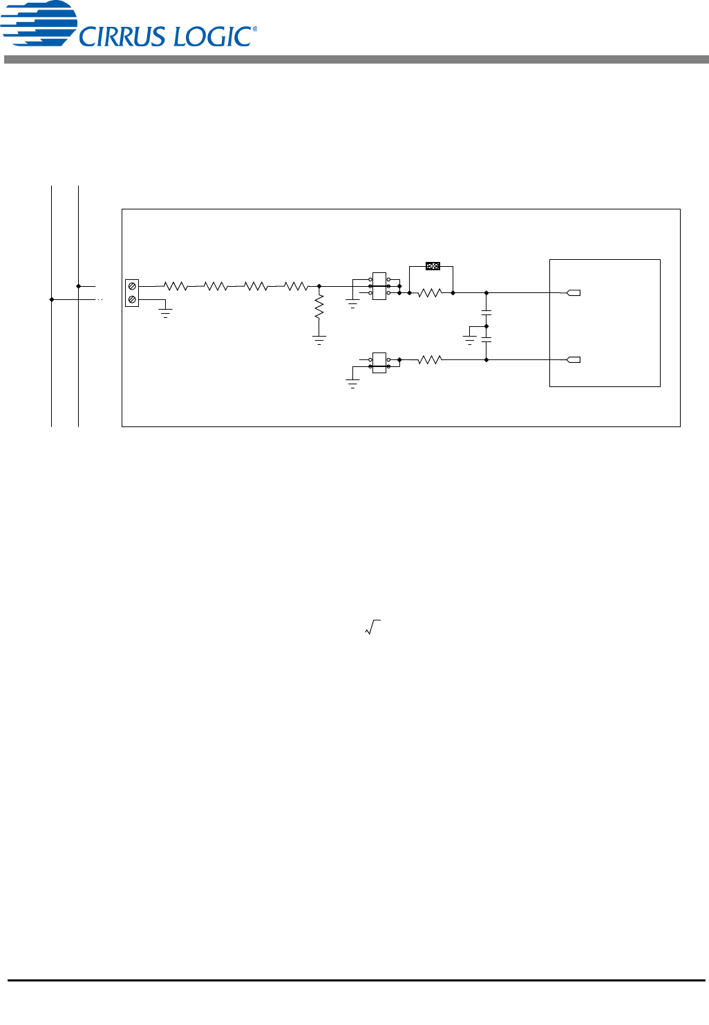
The CDB5480U evaluation board provides screw-type terminal (J4) to connect to the high-voltage line
input. By installing jumpers on J6 to position LINE and J11 to position GND, the input voltage signal is
supplied from the high-voltage input. Extreme care should be used when connecting high-voltage signals
to the CDB5480U evaluation board (see Figure 3).
Figure 3. Voltage Channel — High-voltage Input
The on-board attenuation network provides the following attenuation:
With the CS5480 input range of 250mVp at maximum AC line input of:
is acceptable. It is recommended to apply a 10% margin for the AC line input (270V
rms
).
The CDB5480U evaluation board provides input shorting options for calibration and noise performance
measurements. With a jumper on J6 and J11 in the GND position, the inputs are connected to analog
ground (GND).
GND
LINE
CS5480
CDB5480U
NEUTRAL
LINE
J4
J11
J6
R5
1K
C9
0.027UF
C4
0.027UF
R7
1K
R6
1K
R8
422K
R12
422K
R14
422K
R15
422K
J45
VIN-
VIN+
1k
4 422k1k+
----------------------------------------
1
1689
-------------
=
300V
rms
250mVp
2
-----------------------
1689=