
User Manual


Table Of Contents
- Features
- Table of Contents
- List of Figures
- 1. Hardware
- 2. Software
- 2.1 Installation Procedure
- 2.2 Using the Software
- 2.3 Start-up Window
- 2.4 Connect Menu
- 2.5 System Menu
- 2.5.1 Setup Window
- 2.5.1.1 Refresh Screen Button
- 2.5.1.2 Reset DUT Button
- 2.5.1.3 Save Config and Load Config Buttons
- 2.5.1.4 CS5480 MCLK Frequency
- 2.5.1.5 Configuration Registers
- 2.5.1.6 Pulse Control Register
- 2.5.1.7 Pulse Width and Pulse Rate Registers
- 2.5.1.8 Phase Compensation
- 2.5.1.9 Integrator Gain, System Gain
- 2.5.1.10 Sample Count, Cycle Count, Settle Time
- 2.5.1.11 Epsilon
- 2.5.1.12 ZXNUM
- 2.5.1.13 Mask Register
- 2.5.1.14 Temperature Registers
- 2.5.1.15 Zero-crossing Level and No Load Threshold
- 2.5.1.16 V1/V2 Sag, V1/ V2 Swell, and I1/I2 Overcurrent Registers
- 2.5.1.17 Channel Selection Level, Channel Select Minimum Amplitude, and Voltage Fixed RMS Reference Registers
- 2.5.1.18 Register Checksum, SerialCtrl Registers
- 2.5.1 Setup Window
- 2.6 Calibration Window
- 2.7 Conversion Window
- 2.8 Cirrus Test Window
- 2.8.1 Data Collection Window
- 2.8.1.1 Time Domain / FFT/ Histogram Selector
- 2.8.1.2 Config Button
- 2.8.1.3 Collect Button
- 2.8.1.4 Output Button
- 2.8.1.5 Zoom Button
- 2.8.1.6 Channel Select Button
- 2.8.1.7 Output Button & Window
- 2.8.1.8 Configuration Window
- 2.8.1.9 Collecting Data Sets
- 2.8.1.10 Analyzing Data
- 2.8.1.11 Histogram Information
- 2.8.1.12 Frequency Domain Information
- 2.8.1.13 Time Domain Information
- 2.8.2 Data Collection to File Window
- 2.8.3 Setup and Test Window
- 2.8.1 Data Collection Window
- Appendix A. Bill Of Materials
- Appendix B. Schematics
- Appendix C. Layer Plots
CDB5480U
DS893DB5 5
1.3 Analog Section
The analog section of the CDB5480U is highly configurable. Onboard signal conditioning options for the
voltage and current channels enable most applications to interface directly to the sensors. The following
two sections define the voltage and current channels configurations.
1.3.1 Voltage Sensor Connection
There are three input signal options for the voltage channel input (VIN±): an external low-voltage signal
(via screw terminals or XLR connections), high-voltage line input, or GND. Table 1 illustrates the options
available.
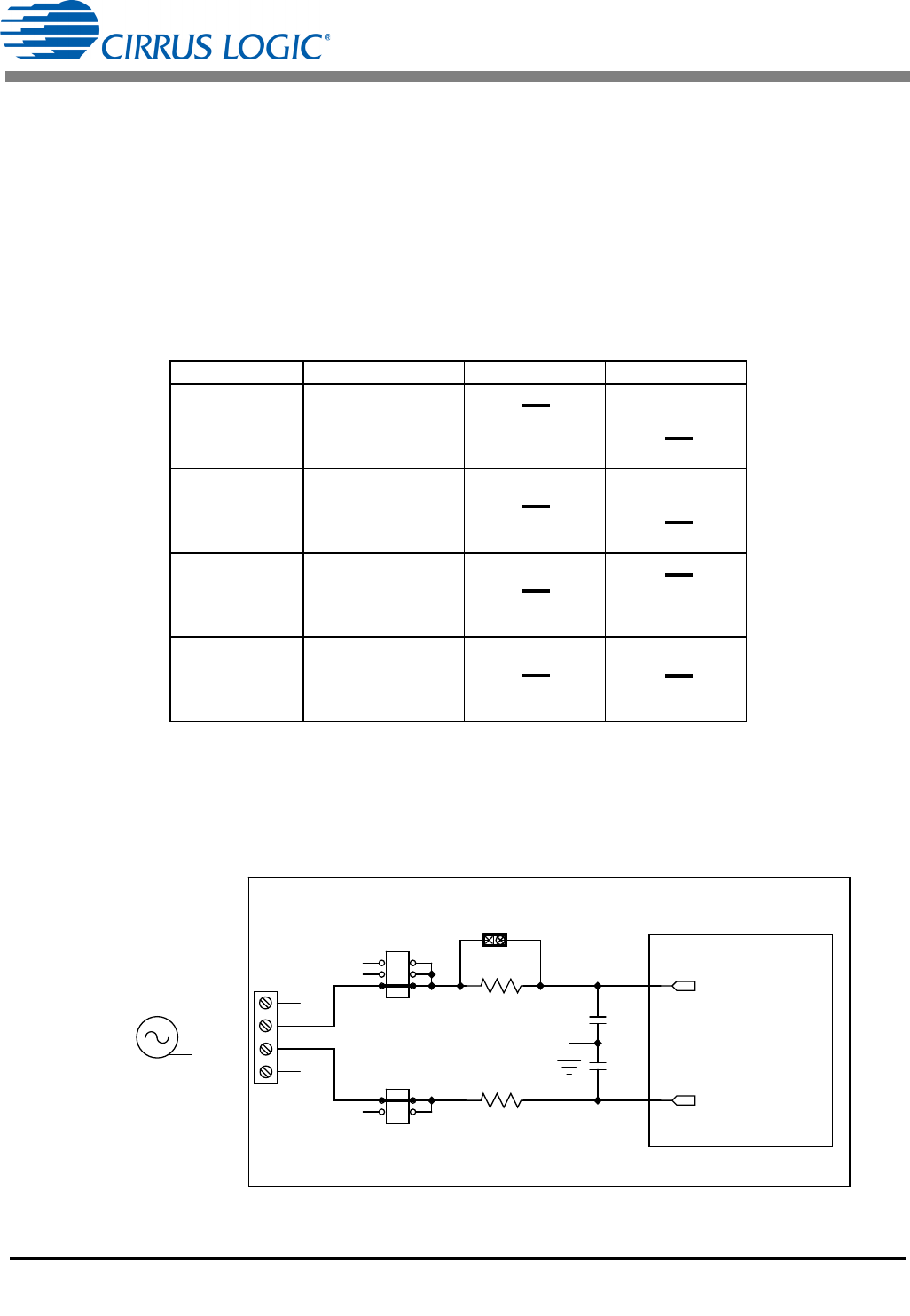
The CDB5480U evaluation board provides screw-type terminals (J3) or XLR connectors (J30) to connect
the low-voltage input signal to the voltage channel (see Figure 2). The screw terminals are labeled as
VIN+ / VIN-. An R-C network at the channel input provides a simple configurable anti-alias filter. By
installing jumpers on J6 to position VIN+ and J11 to position VIN-, the input voltage signal is supplied from
the screw terminals or XLR connection.
Figure 2. Voltage Channel — Low-voltage Input
Table 1. Voltage Channel Input Signal Selection
INPUT Description J11 J6
VIN±
Selects External
Low-voltage Fully
Differential Signal
VIN±
Selects External
Low-voltage Sin-
gle-ended Signal
GND
Selects Grounding
the Input
High Voltage
Line
Selects External
High-voltage AC
Line Signal
O VIN-
O O VIN-
GND
VIN-
(Default)
O VIN+
O O VIN+
O O VIN+
GND
Line
VIN+
(Default)
O VIN-
O O VIN-
GND
VIN-
O VIN+
O O VIN+
O O VIN+
GND
Line
VIN+
O VIN-
O O VIN-
GND
VIN-
O VIN+
O O VIN+
O O VIN+
GND
Line
VIN+
O VIN-
O O VIN-
GND
VIN-
O VIN+
O O VIN+
O O VIN+
GND
Line
VIN+
VIN+
VIN-
250 mVp
CDB5480U
CS5480
J3
J6
J11
C4
0.027UF
C9
0.027UF
R6
1K
R7
1K
J45
VIN+
VIN-