
User Manual


Table Of Contents
- Features
- Table of Contents
- List of Figures
- 1. Hardware
- 2. Software
- 2.1 Installation Procedure
- 2.2 Using the Software
- 2.3 Start-up Window
- 2.4 Connect Menu
- 2.5 System Menu
- 2.5.1 Setup Window
- 2.5.1.1 Refresh Screen Button
- 2.5.1.2 Reset DUT Button
- 2.5.1.3 Save Config and Load Config Buttons
- 2.5.1.4 CS5480 MCLK Frequency
- 2.5.1.5 Configuration Registers
- 2.5.1.6 Pulse Control Register
- 2.5.1.7 Pulse Width and Pulse Rate Registers
- 2.5.1.8 Phase Compensation
- 2.5.1.9 Integrator Gain, System Gain
- 2.5.1.10 Sample Count, Cycle Count, Settle Time
- 2.5.1.11 Epsilon
- 2.5.1.12 ZXNUM
- 2.5.1.13 Mask Register
- 2.5.1.14 Temperature Registers
- 2.5.1.15 Zero-crossing Level and No Load Threshold
- 2.5.1.16 V1/V2 Sag, V1/ V2 Swell, and I1/I2 Overcurrent Registers
- 2.5.1.17 Channel Selection Level, Channel Select Minimum Amplitude, and Voltage Fixed RMS Reference Registers
- 2.5.1.18 Register Checksum, SerialCtrl Registers
- 2.5.1 Setup Window
- 2.6 Calibration Window
- 2.7 Conversion Window
- 2.8 Cirrus Test Window
- 2.8.1 Data Collection Window
- 2.8.1.1 Time Domain / FFT/ Histogram Selector
- 2.8.1.2 Config Button
- 2.8.1.3 Collect Button
- 2.8.1.4 Output Button
- 2.8.1.5 Zoom Button
- 2.8.1.6 Channel Select Button
- 2.8.1.7 Output Button & Window
- 2.8.1.8 Configuration Window
- 2.8.1.9 Collecting Data Sets
- 2.8.1.10 Analyzing Data
- 2.8.1.11 Histogram Information
- 2.8.1.12 Frequency Domain Information
- 2.8.1.13 Time Domain Information
- 2.8.2 Data Collection to File Window
- 2.8.3 Setup and Test Window
- 2.8.1 Data Collection Window
- Appendix A. Bill Of Materials
- Appendix B. Schematics
- Appendix C. Layer Plots
CDB5480U
10 DS893DB5
1.5 Power Supply Selection
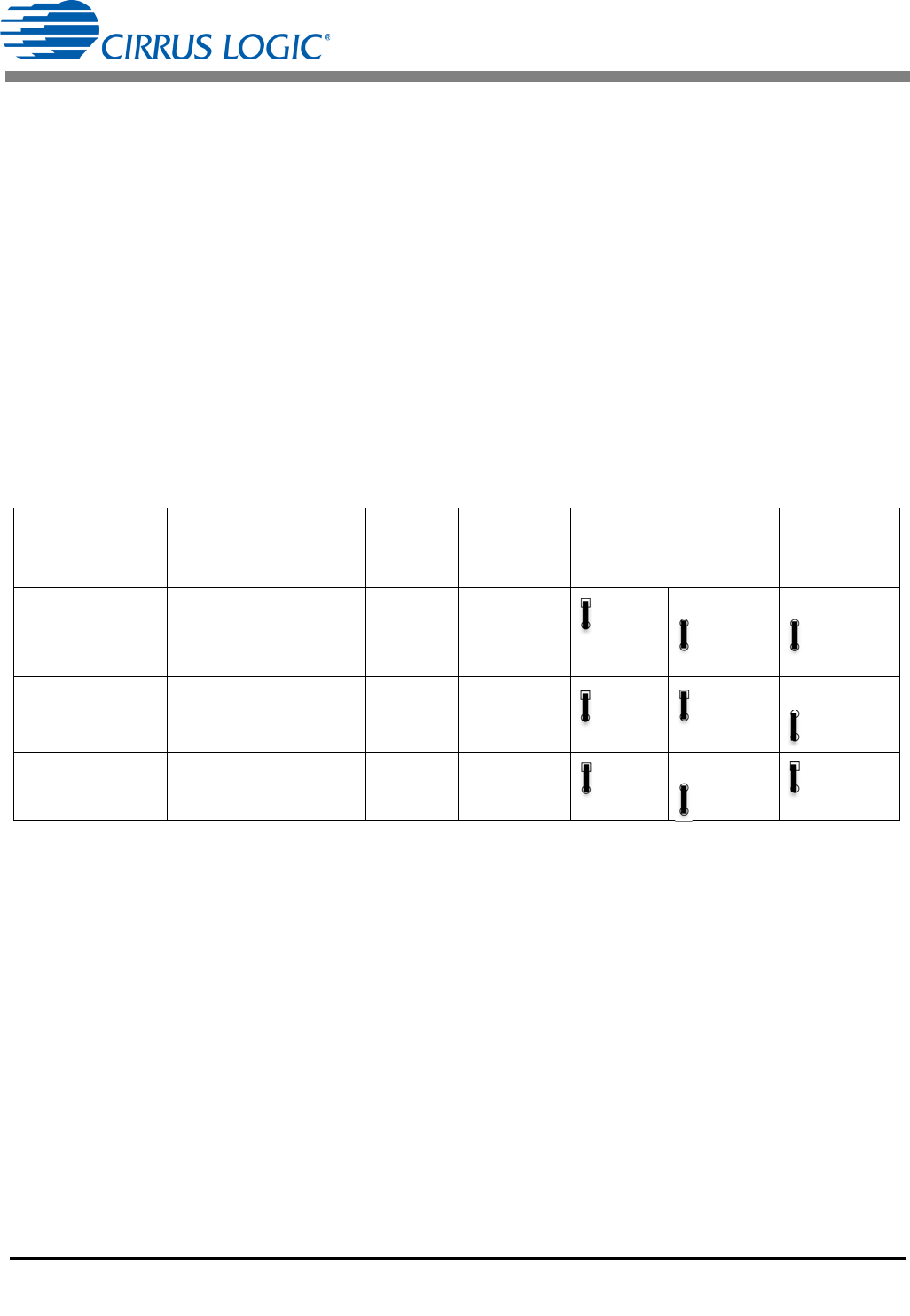
Table 4 illustrates the power supply connections on the evaluation board. The positive analog (VDDA) for
the CS5480 can be supplied using the +3.3V binding post (J36 and J37) or the onboard +3.3V regulator.
Jumper J38 allows the VDDA supply to be sourced from the +3.3V binding post (J37) or the regulated
+3.3V supply. The DC-DC converter (U8) powers the onboard +3.3V regulator. Jumper J26 allows the
+5V supply to be sourced from either the +5V EXT screw connector (J27) or the +5V USB supply. The
+5V supplies the power for the microcontroller (8051_REGIN) and the DC-DC converter (U8). Jumper J21
is used to measure the CS5480 analog supply current and must be installed.
When connecting the CDB5480U board to the AC line through non-isolated sensors, it is strongly
recommended that the CS5480 GND reference is connected to the neutral, the non-isolated current
sensor is connected to the neutral, and the CS5480 is supplied by +3.3V isolated from the AC line. The
DC-DC converter (U8) provides 1kVDC isolation, while no isolation is provided for the 3.3V binding post
connections. If +3.3V is used from the binding post, then the external 3.3VDC power supply must be
isolated from the AC line. To prevent electric shock and damages, always use an isolated power source.
Table 4. Power Supply Selection
6XSS
6RXU
86%
([WHUQDO
86%
([WHUQD
SO\
UFH
&6
6R
%
On
3
Re
O9
%
B
DO9
On
3
reg
6
RXUFH
%L
S
J3
n-board
3.
3 V
egulator
inding
Post
+
n-board
3.3V
gulator
QGLQJ
SRVW
6&J37
8
6X
J
NC +
+3.3 V +
NC N
86%
XSSO\
J24
7HUP
J
+5V N
+5V N
NC +
9
PLQDOV
J27 J
NC
Ƒ
V
ż
V
(de
NC
Ƒ
V
ż
V
+5V
Ƒ
V
ż
V
9''$
J21
VDDA
VDDA
efault)
Ƒ
+
ż
V
ż
+
(d
VDDA
VDDA
Ƒ
+
ż
V
ż
+
VDDA
VDDA
Ƒ
+
ż
V
ż
+
J38
+3.3V
VDDA
+3.3V_2
efault
)
Ƒ
ż
ż
(
+3.3V
VDDA
+3.3V_2
Ƒ
ż
ż
+3.3V
VDDA
+3.3V_2
Ƒ
ż
ż
9B
J26
+5V EXT
+5V
+5V USB
(default)
+5V EXT
+5V
+5V USB
+5V EXT
+5V
+5V USB