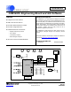
CDB5463U CDB5463U Engineering Board and GUI Software Features General Description The CDB5463U is an inexpensive tool designed to evaluate the functionality and performance of the CS5463 analog-to-digital converter (ADC). The evaluation board includes an LT1019 voltage reference, a C8051F320 microcontroller with a USB interface, and firmware.
CDB5463U TABLE OF CONTENTS 1. HARDWARE ............................................................................................................................. 3 1.1 Introduction ........................................................................................................................ 3 1.2 Evaluation Board Overview ................................................................................................ 3 1.3 Analog Section .........................................................
CDB5463U 1. HARDWARE 1.1 Introduction The CDB5463U evaluation board provides a convenient means of evaluating the CS5463 power measurement IC. The CDB5463U evaluation board operates from a single +5V power supply. The evaluation board interfaces the CS5463 to a PC via a USB cable. To accomplish this, the board comes equipped with a C8051F320 microcontroller and a USB interface. Additionally, the CDB5463U GUI software provides easy access to the internal registers of the CS5463.
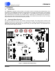
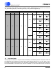
CDB5463U 1.3 Analog Section The CDB5463U evaluation board provides screw-type terminals (J23, J27) to connect input signals to the voltage and current channels. The screw terminals are labels as VIN+, VIN1-, IIN+, and IIN-. A simple R-C network at each channel input provides a simple anti-alias filter. The evaluation board provides three voltage reference options for VREFIN to the CS5463. The three voltage reference options include: VREFOUT from CS5463, the on-board +2.
CDB5463U J26 in the GND position, the inputs are connected to analog ground (AGND). With a jumper on J17, J22, J24 and J26 in position VREF, the inputs are connected to the reference voltage selected on J12.
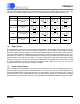
CDB5463U microcontroller (8051_REGIN). Jumper J9 allows the 8051_REGIN supply to be sourced from either the Vu+_EXT binding post (J6), +5V binding post (J3) or VD+_EXT binding post (J5). Power Supplies Power Post Connections Analog (VA+) Digital (VD+) 8051 (Vu+) +5V GND VD+EXT VU+EXT NC VD+ 8051-REGIN J8 J9 VD+_EXT +5 O +3.3 O O O O VD+ VD+ VD+ Vu+_EXT +5 VD+ (Default) NC +5 +5 +5 +5 O O O O O 8051 8051 8051 (Default) +5 VD+_EXT +5 O +3.
CDB5463U between the microcontroller and the CS5463 are removed and the GUI software can not access the CS5463 registers and functions. The EEPROM must be programmed prior to the auto-boot sequence. When the CDB5463U Evaluation Board is sent from the factory, the EEPROM is programmed with the following CS5463 command/data sequence: 1. Write Mode register, turn high-pass filters on: 0x64 0x00 0x00 0x60 2. Unmask bit #2 (LSD) in the Mask register: 0x74 0x00 0x00 0x04 3. Start continuous conversion: 0xE8 4.
CDB5463U 2. SOFTWARE The evaluation board comes with software and an USB cable to link the evaluation board to the PC. The evaluation software was developed with LabWindows®/CVI®, a software development package from national Instruments. The evaluation software is available for download on the Cirrus Logic web site at http://www.cirrus.com/industrialsoftware and was designed to run under Windows® 2000 or Windows XP®. 2.1 Installation To install the software, go to the Cirrus Logic web site at http://www.
CDB5463U 2.3.1 Setup Menu Setup allows user to establish a USB communication connection with CDB5463U board or select a previously saved data file for further analysis. If the USB item in the Setup menu is selected, the evaluation software will poll the CDB5463U, verifying the serial communication link is ready.
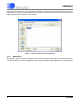
CDB5463U If the Data from Disk item in the Setup menu is selected, a file selection window will appear as shown in Figure 5. User can select a pre-saved data file for further analysis using time domain, FFT, and histogram plots in Data Collection Window of the software. Figure 5. Data from Disc File Selection Window 2.3.
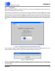
CDB5463U dow. Each window provides a means to evaluate the different functions and performance of the CS5463. Each option has an associated function key (, , etc.). See Figure 6. Figure 6. Menu Pull-down Options 2.3.3 Quit Menu The Quit menu allows the user to exit the evaluation software. Upon selecting Quit, a message window appears and queries if exiting the evaluation software is desired. See Figure 7. Figure 7.
CDB5463U 2.4 Setup Window The evaluation software provides access to the CS5463's internal registers through the Setup window. See Figure 8. The user can enter the Setup window by pulling down the Menu menu and selecting Setup Window, or by pressing on the keyboard. In the Setup window, all of the CS5463's registers are displayed in hexadecimal notation and are decoded to provide easier readability. Refer to the CS5463 data sheet for information on register functionality and definitions.
CDB5463U 2.4.1 Refresh Screen Button The Refresh Screen button will update the contents of the screen by reading all the register values from the CS5463. It is a good idea to press the Refresh Screen button when entering the Setup window, or after modifying any registers, to reflect the current status of the CS5463. 2.4.2 Reset DUT Button The Reset DUT button will hardware reset the CS5463. The CS5463 will perform a reset as discussed in the CS5463 data sheet.
CDB5463U 2.4.8 Control Register The Control Register box contains various bits used to activate or terminate various features of the CS5463. Refer to the CS5463 data sheet for descriptions of the bits. The user is able to turn each bit on or off individually. The value of the Ctrl register is displayed in the HEX: field. Most of the Ctrl register bits are reserved or unused. Only the usable bits are displayed in the Setup window. 2.4.
CDB5463U 2.5.1 Offset / Gain Register In the Offset & Gain fields, the offset and gain registers for both channels are displayed in hexadecimal and decimal formats. These registers can be modified directly by typing the desired value in the hexadecimal display fields. There are two types of offset registers: DC offset and AC offset. The AC Offset register only affects the RMS register values. The DC & AC offset registers are two's complement numbers whose values ranges from -1 to +1.
CDB5463U 2.6 Conversion Window The Conversion Window allows the user to see the results of single and continuous conversions, perform data averaging, and utilize the power-saving modes of the CS5463. See Figure 10. The Conversion Window can be accessed by pulling down the Menu option, and selecting Conversion Window, or by pressing F4. Figure 10. Conversion Window 2.6.1 Single Conversion Button Pressing this button will cause a single conversion to be performed.
CDB5463U 2.6.3 Standby / Sleep Mode Buttons When these buttons are pressed, the CS5463 will enter either standby or sleep power saving modes. To return to normal mode, press the Power Up button. 2.6.4 Power Up Button This button is used to send the Power Up/Halt command to the CS5463. The part will return to normal operating mode and halt any conversions that are being done at this time. 2.6.
CDB5463U 2.7 Pulse Rate Window The CS5463 features a pulse-rate energy output. The CDB5463U has the capability to demonstrate the functionality of this output in the Pulse Rate Output Window. See Figure 11. The Pulse Rate Output Window can be accessed by pressing , or by pulling down the Menu menu, and selecting the Pulse Rate Window item. Figure 11. Pulse Rate Output Window 2.7.1 Integration Seconds This field allows the user to select the length of time over which pulses will be collected.
CDB5463U 2.8 Data Collection Window The Data Collection Window (Figure 12) allows the user to collect sample sets of data from the CS5463 and analyze them using time domain, FFT, and histogram plots. The Data collection Window can be accessed by pulling down the Menu menu, and selecting the Data Collection Window item, or by pressing . Figure 12. Data Collection Window 2.8.
CDB5463U 2.8.5 Zoom Button This button allows the user to zoom in on the plot by selecting two points in the plot area. Press the Restore button to return to the normal data plot, or press the Zoom button again to zoom in even further. 2.8.6 Channel Select Button After data collection, the two buttons labeled as “No Data” will be replaced with Current and Voltage buttons, allowing the user to choose the appropriate channel for display.
CDB5463U 2.8.7.4 Histogram Bin Width This field determines the "bin width" when plotting histograms of the collected data. Each vertical bar in the histogram plot will contain the number of output codes entered in this field. Increasing this number may allow the user to view histograms with larger input ranges. 2.8.7.5 Data to Collect These two check boxes allow the user to select the data types that will be collected and returned to the PC for processing. 2.8.7.
CDB5463U analysis processes acquired conversions to produce a histogram plot. Statistical noise calculations are also calculated and displayed. 2.8.11 Histogram Information The following is a description of the indicators associated with histogram analysis. Histograms can be plotted in the Data Collection Window by setting the analysis type pull-down menu to Histogram. Figure 14. Histogram Analysis 2.8.11.1 BIN Displays the x-axis value of the cursor on the histogram. 2.8.11.
CDB5463U 2.8.11.4 STD_DEV Indicates the standard deviation of the collected data set. The standard deviation is calculated using the following formula: n–1 ∑ ( Xi – MEAN ) STDDEV = 2 i=0 -----------------------------------------------n 2.8.11.5 VARIANCE Indicates for the variance of the current data set. The variance is calculated using the following formula: n–1 ∑ ( Xi – MEAN ) 2 i=0 VARIANCE = -----------------------------------------------n 2.8.11.
CDB5463U 2.8.12 Frequency Domain Information The following describe the indicators associated with FFT (Fast Fourier Transform) analysis. FFT data can be plotted in the Data Collection Window by setting the analysis type selector to FFT (Figure 15). Figure 15. FFT Analysis 2.8.12.1 FREQUENCY Displays the x-axis value of the cursor on the FFT display. 2.8.12.2 MAGNITUDE Displays the y-axis value of the cursor on the FFT display. 2.8.12.3 S/PN Indicates the signal-to-peak noise ratio (decibels). 2.8.12.
CDB5463U 2.8.12.7 FS-Pdb Indicates for the full-scale to signal Ratio (decibels). 2.8.12.8 Time Domain Information The following controls and indicators are associated with time domain analysis. Time domain data can be plotted in the Data Collection Window by setting the analysis type selector to Time Domain (Figure 16). Figure 16. Time Domain Analysis 2.8.12.9 COUNT Displays current x-position of the cursor on the time domain display. 2.8.12.
CDB5463U 2.9 EEPROM Window CDB5463U has an "Auto-Boot" demo feature that uses the on-board serial EEPROM, so that the CDB5463U can operate independently without being connected to a PC. CDB5463U GUI software also provides an EEPROM Window for reading & writing the serial EEPROM (Figure 17). Figure 17. EEPROM Window 2.9.1 Bytes to Read/Write The Bytes to Read/Write field allows the user to define the number of bytes to read or write. 2.9.
CDB5463U 2.10 Debug Panel The Debug panel provides the user a way to access CS5463 registers and send commands to CS5463 directly (Figure 18). Remember that the correct register page must be selected before accessing a register location. Refer to 5.15 in CS5463 data sheet for more details. Figure 18.
Cirrus P/N 001-06872-Z1 001-02779-01 001-02189-Z1 012-00010-Z1 001-04344-01 001-03266-01 001-06685-01 012-00012-01 001-07078-01 070-00055-01 165-00004-01 115-00003-01 110-00041-01 110-00010-01 110-00008-01 115-00016-01 115-00014-01 115-00013-01 110-00056-01 110-00055-01 115-00009-01 115-00031-01 080-00004-01 304-00001-01 020-01848-01 020-01588-01 020-01816-01 020-01930-01 035-00005-01 020-01667-01 020-01905-01 021-00759-01 Item 1 2 3 4 5 6 7 8 9 10 11 12 13 14 15 16 17 18 19 20 21 22 23 24 2
DS805DB2 Cirrus P/N 020-03355-01 020-03378-01 020-03539-01 020-02748-01 020-01473-01 020-02273-Z1 120-00002-01 110-00045-01 062-00124-01 061-00250-01 062-00079-01 060-00061-01 061-00190-01 065-00162-Z3 061-00002-01 061-00219-01 062-00122-01 080-00003-01 300-00001-01 135-00013-01 312-00008-01 100-00049-01 070-00006-01 110-00013-Z1 422-00037-01 240-00176-Z1 603-00176-01 600-00176-01 020-01473-01 110-00045-01 Item 33 34 35 36 37 38 39 40 41 42 43 44 45 46 47 48 49 50 51 52 53 54 55 56 57
CDB5463U Figure 19. Schematic - Analog Inputs APPENDIX B.
Figure 20.
Figure 21.
Figure 22.
CDB5463U Figure 23. Top Silkscreen APPENDIX C.
Figure 24.
Figure 25.
Figure 26.
CDB5463U REVISION HISTORY Revision Date Changes DB1 SEP 2007 Initial Release. DB2 OCT 2007 Minor correction to List of Figures. Contacting Cirrus Logic Support For all product questions and inquiries contact a Cirrus Logic Sales Representative. To find the one nearest to you go to www.cirrus.com IMPORTANT NOTICE Cirrus Logic, Inc. and its subsidiaries ("Cirrus") believe that the information contained in this document is accurate and reliable.