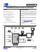
CDB5460AU CDB5460AU Evaluation Board and Software Features General Description The CDB5460AU is an inexpensive tool designed to evaluate the functionality and performance of the CS5460A. The evaluation board includes an LT1019 voltage reference, a C8051F320 microcontroller with a USB interface, and firmware. The microcontroller controls the serial communication between the evaluation board and the PC via the firmware, enabling quick and easy access to all of the CS5460A's registers and functions.
CDB5460AU TABLE OF CONTENTS 1. HARDWARE ............................................................................................................................. 3 1.1 Introduction ........................................................................................................................ 3 1.2 Evaluation Board Overview ................................................................................................ 3 1.3 Analog Section ........................................................
CDB5460AU 1. HARDWARE 1.1 Introduction The CDB5460AU evaluation board provides a quick means of evaluating the CS5460A power measurement IC. The CDB5460AU evaluation board operates from a single +5 V power supply. The evaluation board interfaces the CS5460A to a PC via an USB interface. To accomplish this, the board comes equipped with a C8051F320 microcontroller and a USB interface.
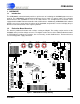
CDB5460AU 1.3 Analog Section The CDB5460AU evaluation board provides screw-type terminals (J23, J27) to connect input signals to the voltage and current channels. The screw terminals are labels as VIN+, VIN-, IIN+, and IIN-. A simple RC network at each channel input provides a simple anti-alias filter. The evaluation board provides three voltage reference options for VREFIN to the CS5460A. The three voltage reference options include: VREFOUT from the CS5460A, the on-board +2.
CDB5460AU are connected to analog ground (AGND). With a jumper on J17, J22, J24, and J26 in position VREF, the inputs are connected to the reference voltage selected on J12.
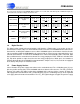
CDB5460AU for the 8051 microcontroller (8051_REGIN). Jumper J9 allows the 8051_REGIN supply to be sourced from either the Vu+_EXT binding post (J6), +5V binding post (J3) or VD+_EXT binding post (J5). Power Supplies Power Post Connections Analog (VA+) Digital (VD+) 8051 (Vu+) +5V GND VD+EXT VU+EXT NC +5 +5 +5 0 8051-REGIN J8 J9 VD+_EXT +5 O +3.3 O O O O VD+ VD+ VD+ Vu+_EXT +5 VD+ (Default) NC +5 VD+ O O O O O 8051 8051 8051 (Default) +5 VD+_EXT +5 O +3.
CDB5460AU The EEPROM must be programmed prior to the auto-boot sequence. When the CDB5460AU Evaluation Board is sent from the factory, the EEPROM is programmed with the following CS5460A command/data sequence: 1. Set Configuration Register, turn high-pass filters on, set K = 1: 0x40 0x00 0x00 0x61 2. Set Pulse_Rate Register to 1000 Hz: 0x4C 0x00 0x7D 0x00 3. Set (Unmask) bit 2 (LSD) in the Mask Register: 0x74 0x00 0x00 0x04 4. Start continuous conversion: 0xE8 5.
CDB5460AU 2. SOFTWARE The evaluation board comes with software and an USB cable to link the evaluation board to the PC. The evaluation software was developed with LabWindows®/CVI®, a software development package from national Instruments. The evaluation software is available for download on the Cirrus Logic web site at http://www.cirrus.com/industrialsoftware and was designed to run under Windows® 2000 or Windows XP®. 2.
CDB5460AU 2.3.1 Setup Menu Setup allows user to establish a USB communication connection with CDB5460AU board or select a previously saved data file for further analysis. If the USB item in the Setup menu is selected, the evaluation software will poll the CDB5460AU, verifying the serial communication link is ready.
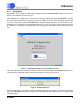
CDB5460AU If the Data from Disk item in the Setup menu is selected, a file selection window will appear as shown in Figure 5. User can select a pre-saved data file for further analysis using time domain, FFT, and histogram plots in Data Collection Window of the software. Figure 5. Data from Disc File Selection Window 2.3.
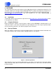
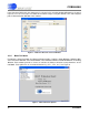
CDB5460AU 2.3.3 Quit Menu The Quit menu allows the user to exit the evaluation software. Upon selecting Quit, a message window appears and queries if exiting the evaluation software is desired. See Figure 7. Figure 7.
CDB5460AU 2.4 Setup Window The evaluation software provides access to the CS5460A's internal registers through the Setup window. See Figure 8. The user can enter the Setup window by pulling down the Menu menu and selecting Setup Window, or by pressing on the keyboard. In the Setup window, all of the CS5460A's registers are displayed in hexadecimal notation and are decoded to provide easier readability. Refer to the CS5460A data sheet for information on register functionality and definitions.
CDB5460AU 2.4.3 CS5460A Crystal Frequency The CS5460A accepts a wide range of crystal input frequencies, and can therefore run at many different sample rates. The crystal frequency being used on the CS5460A should be entered in this box to provide accurate frequency calculation in the FFT window. This will also help the software decide which functions the evaluation system can perform reliably. 2.4.
CDB5460AU 2.5 Calibration Window The Calibration window is used to display and write to the CS5460A offset and gain calibration registers. The user is also able to initiate the CS5460A's calibration sequences that are used to set the calibration values. Both AC and DC calibrations can be run for offset and gain, for either the voltage channel or the current channel, or both simultaneously. The user should refer to the CS5460A data sheet for more details on calibration.
CDB5460AU 2.5.2.1 Offset Calibrations 1. Ground the channel(s) you want to calibrate directly at the channel header(s), J17 and J22 for the voltage channel, J24 and J26 for current channel. The channel(s) could also be grounded directly at the screw-type terminals. 2. Press the corresponding AC or DC offset calibrate button (Cal V, Cal I, or Cal Both) beside or below the offset register fields. 3. The calibration value(s) will automatically update when the calibration is completed. 2.5.2.
CDB5460AU 2.6 Conversion Window The Conversion window allows the user to see the results of single and continuous conversions, perform data averaging, and utilize the power-saving modes of the CS5460A. See Figure 10. The Conversion window can be accessed from the Menu pull-down and selecting Conversion Window, or by pressing . Figure 10. Conversion Window 2.6.1 Single Conversion Button Pressing this button will cause a single conversion to be performed.
CDB5460AU 2.6.4 Power Up Button This button is used to send the Power Up/Halt command to the CS5460A. The part will return to normal operating mode and halt any conversions that are being done at this time. 2.6.5 Write Data to File This box provides a means to write the conversion result data to a .txt text file for later analysis or print out. The file path and name will be shown in Filename field. The Open File button is used to open a new or existing .txt text file for data writing.
CDB5460AU 2.8 Data Collection Window The Data Collection window (Figure 12) allows the user to collect sample sets of data from the CS5460A and analyze them using time domain, FFT, and histogram plots. The Data collection window can be accessed by pulling down the Menu menu, and selecting the Data Collection window item, or by pressing . Figure 12. Data Collection Window 2.8.
CDB5460AU 2.8.4 Output Button This button will bring up a window in which the user can output the collected data to a file for later use, print out a plot, or print out the entire screen. When saving data, only the data channel being displayed on the plot will be saved to a file. 2.8.5 Zoom Button This button allows the user to zoom in on the plot by selecting two points in the plot area. Press the Restore button to return to the normal data plot, or press the Zoom button again to zoom in even further.
CDB5460AU 2.8.7.3 FFT Window This field allows the user to select the type of windowing algorithm for FFT processing. Windowing algorithms include the Blackman, Blackman-Harris, Hanning, 5-term Hodie, and 7-term Hodie. The 5-term Hodie and 7-term Hodie are windowing algorithms developed at Crystal Semiconductor. 2.8.7.4 Histogram Bin Width This field determines the "bin width" when plotting histograms of the collected data.
CDB5460AU 2.8.10 Analyzing Data The evaluation software provides three types of analysis tests: Time Domain, Frequency Domain, and Histogram. The time domain analysis processes acquired conversions to produce a plot of magnitude versus conversion sample number. The frequency domain analysis processes acquired conversions to produce a plot of magnitude versus frequency using the Fast-Fourier transform (results up to Fs/2 are calculated and plotted).
CDB5460AU 2.8.11.3 MEAN Indicates the mean of the data sample set. The mean is calculated using the following formula: n–1 ∑ Xi i=0 Mean = ---------------n 2.8.11.4 STD_DEV Indicates the standard deviation of the collected data set. The standard deviation is calculated using the following formula: n–1 ∑ ( Xi – MEAN ) STDDEV = 2 i=0 -----------------------------------------------n 2.8.11.5 VARIANCE Indicates for the variance of the current data set.
CDB5460AU 2.8.12 Frequency Domain Information The following describe the indicators associated with FFT (Fast Fourier Transform) analysis. FFT data can be plotted in the Data Collection window by setting the analysis type selector to FFT. Figure 15. FFT Analysis 2.8.12.1 FREQUENCY Displays the x-axis value of the cursor on the FFT display. 2.8.12.2 MAGNITUDE Displays the y-axis value of the cursor on the FFT display. 2.8.12.3 S/PN Indicates the signal-to-peak noise ratio (decibels). 2.8.12.
CDB5460AU 2.8.12.6 SNR Indicates for the signal-to-noise ratio, first 4 harmonics are not included (decibels). 2.8.12.7 FS-Pdb Indicates for the full-scale to signal Ratio (decibels). 2.8.12.8 Time Domain Information The following controls and indicators are associated with time domain analysis. Time domain data can be plotted in the Data Collection window by setting the analysis type selector to Time Domain. Figure 16. Time Domain Analysis 2.8.12.
CDB5460AU 2.9 EEPROM Window CDB5460AU has an "Auto-Boot" demo feature that uses the on-board serial EEPROM, so that the CDB5460AU can operate independently without being connected to a PC. CDB5460AU GUI software also provides an EEPROM window for reading & writing the serial EEPROM. Figure 17. EEPROM Window 2.9.1 Bytes to Read/Write The Bytes to Read/Write field allows the user to define the number of bytes to read or write. 2.9.
CDB5460AU 2.10 Debug Panel The Debug panel provides the user a way to access CS5460A registers and send commands to CS5460A directly. See Figure 18. Refer to section 4.1 in the CS5460A data sheet for more detailed information about the commands and registers. Figure 18.
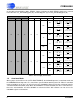
DS487DBU1 Cirrus P/N 001-06872-Z1 001-02779-Z1 001-02189-Z1 012-00010-Z1 001-04344-Z1 001-03266-Z1 001-06685-Z1 012-00012-Z1 001-07078-Z1 070-00055-Z1 165-00004-Z1 115-00003-Z1 110-00041-Z1 110-00010-Z1 110-00008-Z1 115-00016-Z1 115-00014-Z1 115-00013-Z1 110-00056-Z1 110-00055-Z1 115-00009-Z1 115-00031-Z1 080-00004-Z1 304-00001-Z1 020-01848-Z1 020-01588-Z1 020-01816-Z1 020-01930-Z1 035-00005-Z1 020-01667-Z1 020-01905-Z1 021-00759-Z1 Item 1 2 3 4 5 6 7 8 9 10 11 12 13 14 15 16 17 18 19 20 21 22
Cirrus P/N 020-03355-Z1 020-03378-Z1 020-03539-Z1 020-02748-Z1 020-01473-Z1 020-02273-Z1 120-00002-Z1 110-00045-Z1 062-00124-Z1 061-00250-Z1 062-00079-Z1 060-00061-Z1 061-00190-Z1 065-00161-Z2 061-00002-Z1 061-00219-Z1 062-00122-Z1 080-00003-Z1 300-00025-Z1 135-00013-01 100-00049-Z1 070-00006-Z1 600-00176-Z2 240-00176-Z1 603-00176-01 110-00013-Z1 422-00037-01 020-01473-Z1 110-00045-Z1 312-00008-01 Item 33 34 35 36 37 38 39 40 41 42 43 44 45 46 47 48 49 50 51 52 53 54 55 56 57 58 59
CDB5460AU Figure 19. Schematic - Analog Inputs APPENDIX B.
Figure 20.
Figure 21.
Figure 22.
CDB5460AU Figure 23. Top Silkscreen APPENDIX C.
Figure 24.
Figure 25.
Figure 26.
CDB5460AU REVISION HISTORY Revision Date DB1 JAN 2009 DS487DBU1 Changes Initial Release.
CDB5460AU Contacting Cirrus Logic Support For all product questions and inquiries contact a Cirrus Logic Sales Representative. To find the one nearest to you go to www.cirrus.com IMPORTANT NOTICE Cirrus Logic, Inc. and its subsidiaries ("Cirrus") believe that the information contained in this document is accurate and reliable. However, the information is subject to change without notice and is provided "AS IS" without warranty of any kind (express or implied).