
Instruction Manual


4 DS963DB1
CDB53L30
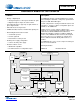
1.4 Serial Audio I/O
1.4 Serial Audio I/O
Header J29 provides an interface for the I
2
S and TDM serial audio clocks and data. The header signals are described in
Table 1-2. MCLK routing is controlled by the settings on the “Board Config” tab in the FlexGUI. The direction of the LRCK/
FSYNC and SCLK pins is configured by the “Serial Header Direction” control on the “Board Config” tab. When configured
as Master, LRCK/FSYNC and SCLK are outputs from the CDB53L30. When configured as Slave, LRCK/FSYNC and
SCLK are inputs to the CDB53L30. The logic level for all serial I/O is +1.8 V.
1.5 S/PDIF Transmitter
The CS8406 S/PDIF transmitter on the CDB53L30 provides a two-channel digital output simultaneously to both the RCA
coaxial connector (J35) and the optical output connector (OPT2). To use the S/PDIF transmitter, the CS53L30 must be
configured for I
2
S mode, and the CS53L30 MCLK/LRCK ratio must correspond to one of the four ratios supported by the
CS8406: 128x, 256x, 384x, or 512x. Only one SDOUT signal may be chosen for output at any time. The CS8406 clock
ratio and desired SDOUT signal are selected on the “Board Config” tab of the FlexGUI.
1.6 Master Clock
The CDB53L30 includes a fixed-frequency crystal oscillator and CS2300 programmable PLL, facilitating the generation of
an onboard MCLK. The MCLK frequency is configured on the “Board Config” tab of the FlexGUI.
Table 1-1. Digital Microphone Connections to the Input Header
Header Pin Direction Description
1.SCLK1 Output Digital mic 1 serial clock from CS53L30 #1
1.SCLK2 Output Digital mic 2 serial clock from CS53L30 #1
2.SCLK1 Output Digital mic 1 serial clock from CS53L30 #2
2.SCLK2 Output Digital mic 2 serial clock from CS53L30 #2
1.DATA1 Input Digital mic 1 data to CS53L30 #1
1.DATA2 Input Digital mic 2 data to CS53L30 #1
2.DATA1 Input Digital mic 1 data to CS53L30 #2
2.DATA2 Input Digital mic 2 data to CS53L30 #2
1.BIAS1 Output Mic bias 1 from CS53L30 #1 (To supply bias directly to the pin with no series bias
resistor, the “Rbias SHORT” pin jumper should be shunted)
1.BIAS3 Output Mic bias 3 from CS53L30 #1 (To supply bias directly to the pin with no series bias
resistor, the “Rbias SHORT” pin jumper should be shunted)
2.BIAS1 Output Mic bias 1 from CS53L30 #2 (To supply bias directly to the pin with no series bias
resistor, the “Rbias SHORT” pin jumper should be shunted)
2.BIAS3 Output Mic bias 3 from CS53L30 #2 (To supply bias directly to the pin with no series bias
resistor, the “Rbias SHORT” pin jumper should be shunted)
Table 1-2. Serial Header Signal Descriptions
Header Pin Direction Description
MCLK IN Input Master clock input
MCLK OUT Output Master clock output
SCLK Input/Output I
2
S or TDM bit clock
LRCK/FSYNC Input/Output I
2
S left/right clock or TDM frame sync
1.ASP1_SDOUT Output ASP1_SDOUT I
2
S or TDM data from CS53L30 #1;
In I
2
S mode, left channel corresponds to 1.AIN1, right channel corresponds to 1.AIN2.
In TDM mode, channel slot location is configurable.
1.ASP2_SDOUT Output ASP2_SDOUT I
2
S data from CS53L30 #1;
Left channel corresponds to 1.AIN3, right channel corresponds to 1.AIN4.
2.ASP1_SDOUT Output ASP1_SDOUT I
2
S or TDM data from CS53L30 #2;
In I
2
S mode, left channel corresponds to 2.AIN1, right channel corresponds to 2.AIN2.
In TDM mode, channel slot location is configurable.
2.ASP2_SDOUT Output ASP2_SDOUT I
2
S data from CS53L30 #2;
Left channel corresponds to 2.AIN3, right channel corresponds to 2.AIN4.