CDB53L30 Evaluation Board for the CS53L30 Features Description • Analog or digital Inputs The CDB53L30 board is a dedicated platform for testing and evaluating the CS53L30, a low-power, quad-channel microphone ADC with TDM output. — Analog microphone or line inputs via TRS 1/8” jacks — Digital microphone inputs via stake headers To allow comprehensive testing of CS53L30 features and performance, extensive software-configurable options are available on the CDB53L30.
CDB53L30 Table of Contents 1 The CDB53L30 System Overview . . . . . . . . . . . . . . . . . . . . . . . 1.1 Power Supply Circuitry . . . . . . . . . . . . . . . . . . . . . . . . . . . . . 1.2 Analog Inputs . . . . . . . . . . . . . . . . . . . . . . . . . . . . . . . . . . . . 1.3 Digital Mic Inputs . . . . . . . . . . . . . . . . . . . . . . . . . . . . . . . . . . 1.4 Serial Audio I/O . . . . . . . . . . . . . . . . . . . . . . . . . . . . . . . . . . . 1.5 S/PDIF Transmitter . . . . . . . . . . . . . .
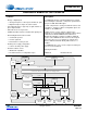
CDB53L30 1 The CDB53L30 System Overview 1 The CDB53L30 System Overview The CDB53L30 evaluation board is a convenient platform for evaluating the CS53L30 low-power, quad-channel microphone ADC with TDM output. It supports multiple power supply and signal I/O configurations, including the option to connect directly to the CS53L30 from an external system such as a host processor (while bypassing the onboard control circuitry).
CDB53L30 1.4 Serial Audio I/O Table 1-1. Digital Microphone Connections to the Input Header Header Pin Direction Description 1.SCLK1 Output Digital mic 1 serial clock from CS53L30 #1 1.SCLK2 Output Digital mic 2 serial clock from CS53L30 #1 2.SCLK1 Output Digital mic 1 serial clock from CS53L30 #2 2.SCLK2 Output Digital mic 2 serial clock from CS53L30 #2 1.DATA1 Input Digital mic 1 data to CS53L30 #1 1.DATA2 Input Digital mic 2 data to CS53L30 #1 2.DATA1 Input Digital mic 1 data to CS53L30 #2 2.
CDB53L30 1.7 Synchronization I/O The Serial Audio I/O header J29 provides a MCLK input pin and MCLK output pin. The MCLK IN pin can be used to provide an externally generated MCLK to the board. The MCLK OUT pin provides either a buffered version of the onboard generated MCLK or a buffered version of the MCLK IN signal. By providing a buffered version of the MCLK IN signal, the MCLK OUT pin may be used for daisy chaining an additional CDB53L30.
CDB53L30 2 Quick-Start Guide 2 Quick-Start Guide This section describes a basic setup procedure for the CDB53L30. After completing the steps in Fig. 2-1, the CDB53L30 will be configured to accept eight single-ended or differential analog line inputs and will output four two-channel I2S streams at a sample rate of 48 kHz. 5 1 2 3 Return Returnallalljumpers jumperstotodefault the factory factory settings. See See default settings. Table 3-1.3-1. Table3-2 3-2and andFig.
CDB53L30 3 System Connections and Jumper Settings Table 2-1. Quick-Start Serial Header Signal Descriptions (Cont.) Header Pin 1.ASP2_SDOUT Direction Output 2.ASP1_SDOUT Output 2.ASP2_SDOUT Output Frequency Description N/A ASP2_SDOUT I2S data from CS53L30 #1; Left channel corresponds to 1.AIN3, right channel corresponds to 1.AIN4 N/A ASP1_SDOUT I2S data from CS53L30 #2; Left channel corresponds to 2.AIN1, right channel corresponds to 2.
CDB53L30 3 System Connections and Jumper Settings Table 3-2. CDB53L30 Jumper Settings (Cont.) Jumper Pin Block Connection Purpose J34 CONTROL Gang control signals of SHORTS CS53L30 #1 and CS53L30 #2 J39, J44, J45, J86, Rbias Shunt across the J73, J78, J51, J46 SHORT 1.
CDB53L30 3 System Connections and Jumper Settings Figure 3-1.
CDB53L30 4 Software Control Using FlexGUI 4 Software Control Using FlexGUI The Cirrus Logic FlexGUI application is a graphical user interface that allows users to easily configure software modifiable options on the CDB53L30, such as the register settings of the CS53L30 and the CS8046 S/PDIF transmitter. 4.1 Installation and First-Time Setup To set up FlexGUI for use with the CDB53L30, follow these steps: 1. Download the latest version of the FlexGUI control software from www.cirrus.com/msasoftware.
CDB53L30 4.3 Using the FlexGUI Tabs To restore one of several standard configurations predefined at the factory, use the Quick Setup drop-down box on the “Board Config” tab, or use the Restore Board Registers... command to load any of the configurations starting with “FACTORY--” in the file name. The file names are meant to be self-explanatory. For example, the script called “FACTORY--analog_48k_12.288M_master_I2S_dual.fgs” configures the board as I2S master with a 48k sample rate and 12.
CDB53L30 4.3 Using the FlexGUI Tabs 4.3.1 Board Config Tab The “Board Config” tab contains the controls for configuring the MCLK source, S/PDIF transmitter, serial header, and CS53L30 mute signals. The individual functions of this tab are described below. • Quick Setup—Drop-down box for selecting a factory preset register configuration. • MCLK—Settings for onboard MCLK frequency and MCLK routing. • S/PDIF Transmitter—Settings for the CS8406 S/PDIF transmitter. See Section 1.5 for more information.
CDB53L30 4.3 Using the FlexGUI Tabs 4.3.2 CS53L30 Config Tab The “CS53L30-1 Config” and “CS53L30-2 Config” tabs contain the controls for configuring the CS53L30 power down state, serial port settings, DMIC, mic bias, input pin bias, MUTE pin power down behavior, and multichip synchronization. • Power—Configures the power down controls and supply settings. • MCLK—Controls for MCLK configuration. • ASP—Settings for Audio Serial Port configuration. • DMIC—Settings for digital mic configuration.
CDB53L30 4.3 Using the FlexGUI Tabs 4.3.3 CS53L30 ADC Tab The “CS53L30-1 ADC” and “CS53L30-12 ADC” tabs contain the controls for the ADC settings, including notch filter enable, high-pass filter configuration, noise gating, volume controls, and input type. The controls on the left correspond to ADC1, and the controls on the right correspond to ADC2. • Disable digital notch filter—Disables the digital notch filter (applies to both channels of the ADC).
CDB53L30 4.3 Using the FlexGUI Tabs 4.3.4 CS53L30 TDM Tab The “CS53L30-1 TDM” and “CS53L30-2 TDM” tabs contain the controls for configuring the CS53L30 TDM output. These controls apply only when the ASP Mode is configured for TDM on the “CS53L30 Config” tab. • Shift TDM frame 1/2 SCLK left—Configures the start offset of TDM data after a rising edge of LRCK/FSYNC. • LRCK Pulse Width—Configures the LRCK/FSYNC high time in TDM mode.
CDB53L30 4.4 Register Maps Tab 4.4 Register Maps Tab The “Register Maps” tab shows the entire user configurable register space for all programmable devices on the CDB53L30. It is especially useful for reading/writing a device’s register settings directly, one register at a time. For example, the default value for register 0x10 is 0x2F (Figure 4-8). To modify register 0x10’s value, first navigate to it by locating the cell at the intersection of row “10” and column “00.
CDB53L30 5 Performance Plots 5 Performance Plots Test conditions (unless otherwise specified): FSext = 48 kHz; MCLKext = 12.2880 MHz; preamp setting: 0 dB (bypassed); PGA setting: 0 dB; high-pass filter enabled, ADCx_HPF_CF = 00; notch filter disabled; noise gate disabled; MCLK autoscale enabled; VA = 1.8 V, VP = 3.6 V. THD+N measurement bandwidth = 10 Hz to FSext/2, no weighting. Unless otherwise specified, the performance data is representative of all channels on both CS53L30 devices.
CDB53L30 5 Performance Plots G % ) 6 G % ) 6 N N N N N +] G % ) 6 N N N N N Figure 5-7. Output FFT, 1 kHz, –60 dBFS Note: The low-frequency roll-off is due to the corner frequency set by the DC blocking cap (0.
CDB53L30 5 Performance Plots 7 G % ) 6 G % ) 6 7 N N N N N N Figure 5-11. Frequency Response, Notch Filter Disabled, Preamp Enabled (+10 dB or +20 dB), –1 dBFS N N 7 7 G % ) 6 Note: The low-frequency roll-off is due to the corner frequency set by the DC blocking cap (0.1 F) and the input impedance (50 k when the preamp setting is 0 dB).
CDB53L30 5 Performance Plots Note: The low-frequency distortion is dominated by the MLCC Class II DC blocking capacitor (0.1 F). To reduce this distortion, reduce the corner frequency by selecting a larger cap, or choose a different cap type such as film or MLCC Class I.
CDB53L30 5 Performance Plots G % G % G%U G%U Figure 5-23. THD+N (Relative) vs. Level, Preamp Setting: +10 dB, PGA Setting: +12 dB, 1 kHz Figure 5-24. THD+N (Relative) vs.
CDB53L30 6 Schematics 6 Schematics CS53L30-1 TP12 1.ASP1_SDOUT VA TP13 1.SCLK I2C Address: 0x90 R22 NO POP CS53L30-1.DMIC1_SCLK R34 0 R36 0 [2] 0 R62 0 CS53L30-1.ASP1_SDOUT [4] TP42 1.MCLK TP17 1.DMIC1_SCLK [2] CS53L30-1.DMIC2_SCLK/AD1 R59 CS53L30-1.SCLK [4] CS53L30-1.MCLK [3] VA CS53L30.I2C.SDA [2,5] CS53L30.I2C.SCL [2,5] TP19 1.DMIC2_SCLK/AD1 R23 10K R21 NO POP CS53L30-1.IN1+ CS53L30-1.IN1CS53L30-1.IN2+ CS53L30-1.IN2CS53L30-1.IN3+ CS53L30-1.IN3CS53L30-1.IN4+ CS53L30-1.
CDB53L30 6 Schematics CS53L30-1 Input 1 (Analog/Digital) 1.AIN1 T R Input 2 (Analog) 1.AIN2 4 2 6 CS53L30-1.MIC1_BIAS 5 3 Rbias CK-3.5-027A J53 AINSleeve J6 HDR5X2 1 2 3 4 5 6 7 8 9 10 R27 1.8K J39 J36 [2] R Rbias Short (Jumper) J38 C20 C78 0.1uF X5R 0.1uF X5R CS53L30-1.IN1+ [2] T R CS53L30-1.IN1- [2] 1.AIN4 5 3 J19 HDR5X2 1 2 3 4 5 6 7 8 9 10 Rbias Short (Jumper) Bias to AIN+ (Jumper) J43 C21 1.AIN2+ 1.AIN21.BIAS2 C22 0.1uF X5R 0.1uF X5R CS53L30-1.IN2+ [2] CS53L30-1.
CDB53L30 6 Schematics Master Clock PLL +3.3V I2C Address: 0x9C +3.3V C133 X5R 0.1uF C134 X5R 1uF 6.3V R143 0 NO POP To MCLK routing buffers [3] PLL.CLK_OUT1 R74 22.1 [3] PLL.CLK_OUT2 R70 22.1 PLL_AUX_OUT +3.3V R14 U15 CS2300CP-CZZ 1 2 3 4 5 22.1 SDA/CDIN SCL/CCLK AD0/CS FILTN FILTP VD GND CLK_OUT AUX_OUT CLK_IN 10 9 8 7 6 R104 R136 0 0 C135 X5R 0.1uF UC.I2C.SDA [4,5] UC.I2C.SCL [4,5] R142 0 L1 600OHM@100MHZ R255 0 Y1 24.576MHZ 1 3 TRI-S OUT 4 VDD 2 C85 X5R 1uF 6.3V R200 22.
CDB53L30 6 Schematics Serial Audio Header VA +1.8V R85 NO POP R92 +1.8V R126 10K 0 0 R94 C56 X5R 0.1uF 0 C55 X5R 0.1uF R44 0 NO POP 3 NTR4501NT1G [2] CS53L30-1.SCLK R76 0 [2] CS53L30-2.SCLK R77 0 [4] SPDIF_TX.SCLK R162 0 [2] CS53L30-1.LRCK/FSYNC [2] CS53L30-2.LRCK/FSYNC R78 0 R79 0 0 [4] SPDIF_TX.LRCK R164 [3] PLL.LRCK_IN R135 0 U21 1 VCCA 2 A1 3 A2 4 GND 1 8 VCCB 7 B1 6 B2 5 DIR R91 R90 0 0 2 SERIAL_HDR.M/S [5] Q1 R125 10K SN74LVC2T45DCUR VA +1.
VA VA NO POP 0 0 R49 R50 NO POP 0 0 SPDIF_TX.LRCK SPDIF_TX.SCLK R82 R55 C14 X5R 0.1uF C33 X5R 0.1uF VA R10 R31 NO POP 0 0 C12 X5R 0.1uF [2,4] CS53L30-2.ASP1_SDOUT [2,4]CS53L30-2.ASP2_SDOUT/AD0 +1.8V [2,4] CS53L30-1.ASP1_SDOUT [2,4] CS53L30-1.ASP2_SDOUT/AD0 +1.8V [4] [4] +1.
CDB53L30 6 Schematics Microcontroller +3.3V +3.3V +3.3V C83 X5R 4.7UF C82 X5R 4.7UF C84 X5R 0.1uF C118 X5R 0.1uF R39 1K SERIAL_HDR.M/S [4] R38 1K U7 6 [3] HDR_MCLK_OUT_EN To MCLK [3] PLL_MCLK_OUT_EN Routing Buffers [3] HDR_MCLK_IN_EN [3] PLL_MCLK_EN [4] To SPDIF SDIN Mux R32 R33 R108 R109 R110 R111 R112 R113 SPDIF_TX.RST 18 17 16 15 14 13 12 11 0 0 0 0 0 0 0 0 REGIN P0.1 P0.0 P0.2 P0.3 P0.4 P0.5 P0.6 P0.7 10 P3.0/C2D 9 RST/C2CK [4] SPDIF_TX.SDIN_SEL0 [4] SPDIF_TX.SDIN_SEL1 P1.0 P1.1 P1.
CDB53L30 6 Schematics Level Shifters and Control I/O Header VA R153 11.5K 1% NO POP [5] UC.SW/HW OE1 [5] 2 UC.CS53L30-1.RESET +1.8V 1 A1 Y1 6 R145 0 R147 NO POP Optional Voltage Supervisor R144 11.5K 1% +3.3V +3.3V U24 MIC2774L-31YM5 0 R151 10K U27-B 1 NC7WZ126K8X 4 VDD RST MR IN [5] UC.SW/HW 5 3 GND OE2 5 [5] UC.CS53L30-2.RESET 7 A2 Y2 3 R146 0 R148 NO POP R154 2.49K 1% 0 U27-C 0805 VTH= 1.69V NC7WZ126K8X +1.8V +3.3V V 8 C81 X5R 0.
CDB53L30 6 Schematics Power Supply Binding Posts +5V_EXT +5V J83 1 +5V_EXT 1 J89 2 [5] TP18 +5V USB.VBUS C244 TANT 100uF 10V Z4 P6SMB6.8AT3G 6.8Vbr J31 1 GND VA_EXT J9 1 J1 2 VA +1.8V 1 VA_EXT C3 TANT 100uF 10V Z1 P6SMB6.8AT3G 6.8Vbr R3 TP1 VA 1 current sense J2 VP_EXT J14 1 J8 2 VP +3.6V 1 VP_EXT VP I-SENSE C1 TANT 100uF 10V Z3 P6SMB6.8AT3G 6.8Vbr R4 TP3 VP 1 current sense J13 +5.0V to +3.
CDB53L30 7 Layout 7 Layout Figure 7-1.
CDB53L30 7 Layout Figure 7-2.
CDB53L30 7 Layout Figure 7-3.
CDB53L30 7 Layout Figure 7-4. Layer 3 (+3.3 V, +1.
CDB53L30 7 Layout Figure 7-5.
CDB53L30 7 Layout Figure 7-6.
CDB53L30 7 Layout Figure 7-7.
CDB53L30 8 Revision History 8 Revision History Release DB1 Changes Initial Release Contacting Cirrus Logic Support For all product questions and inquiries, contact a Cirrus Logic Sales Representative. To find the one nearest you, go to www.cirrus.com. IMPORTANT NOTICE Cirrus Logic, Inc. and its subsidiaries ("Cirrus") believe that the information contained in this document is accurate and reliable.