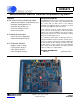
CDB5374 Multichannel Marine Seismic Evaluation System Features General Description z The CDB5374 board is used to evaluate the functionality and performance of the Cirrus Logic multichannel marine seismic chip set. Data sheets for the CS5374, CS5376A, and CS4373A devices should be consulted when using the CDB5374 evaluation board.
CDB5374 REVISION HISTORY Revision Date DB1 JAN 2009 Changes Initial release. Contacting Cirrus Logic Support For all product questions and inquiries contact a Cirrus Logic Sales Representative. To find the one nearest to you go to www.cirrus.com IMPORTANT NOTICE Cirrus Logic, Inc. and its subsidiaries ("Cirrus") believe that the information contained in this document is accurate and reliable.
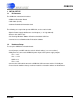
CDB5374 TABLE OF CONTENTS REVISION HISTORY .................................................................................................................... 2 1. INITIAL SETUP ......................................................................................................................... 5 1.1 Kit Contents ....................................................................................................................... 5 1.2 Hardware Setup ...................................................
CDB5374 3.4.2 Statistics .............................................................................................................. 46 3.4.3 Plot Enable .......................................................................................................... 46 3.4.4 Cursor ................................................................................................................. 47 3.4.5 Zoom ........................................................................................................
CDB5374 1. INITIAL SETUP 1.1 Kit Contents The CDB5374 evaluation kit includes: • CDB5374 Evaluation Board • USB Cable (A to B) • Software Download Information Card The following are required to operate CDB5374, and are not included: • Bipolar Power Supply with Banana Jack Outputs (+/-12 V @ 300 mA) • Banana Jack Cables (4x) • PC Running Windows 2000 or XP with an Available USB Port • Internet Access to Download the Evaluation Software 1.
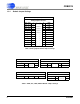
CDB5374 1.2.1 Default Jumper Settings J27, J227, J327, J427 CH1, CH2, CH3, CH4 Analog Input Selections DAC_OUT+ 1 * * 2 INA+ DAC_OUT- 3 * * 4 INA- DAC_OUT- 5 ---------- 6 INB- DAC_OUT+ 7 ---------- 8 INB+ DAC_BUF+ 9 ---------- 10 INA+ DAC_BUF- 11 ---------- 12 INA- DAC_BUF- 13 * * 14 INB- DAC_BUF+ 15 * * 16 INB+ BNC_IN+ 17 * * 18 INA+ BNC_IN- 19 * * 20 INA- BNC_IN- 21 * * 22 INB- BNC_IN+ 23 * * 24 INB+ Table 1.
CDB5374 J10 J11 VA- Voltage Selection VA+ Voltage Selection -2.5VA 1 ---------- 2 GND 3 * * 4 EXT_VA- 5 * * 6 +2.5VA 1 ---------- 2 +5VA 3 * * 4 EXT_VA+ 5 * * 6 J12 J13 VD Input Voltage Source VCORE Input Voltage Source EXT_VA+ 1 * * 2 EXT_VA+ 1 * * 2 EXT_VD 3 ---------- 4 EXT_VD 3 ---------- 4 J22 J21 VD Voltage Selection VCORE Voltage Selection +3.3VD 1 ---------- 2 EXT_VD 3 * 4 * +3.3VD 1 ---------- 2 +2.
CDB5374 J15 J14 I2C Data I2C Clock SDA+ 1 * * 2 SCL+ 1 * * 2 SDA- 3 * * 4 SCL- 3 * * 4 SDA 5 * * 6 SCL 5 * * 6 GND 7 * * 8 GND 7 * * 8 J23 I2C Clock Driver Enable GND 1 ---------- 2 VD 3 * * 4 J24 J25 Clock Source Sync Source CLK+ 1 * * 2 SYNC+ 1 * * 2 CLK- 3 * * 4 SYNC- 3 * * 4 CLK_I/O 5 * * 6 SYNC_I/O 5 * * 6 GND 7 * * 8 GND 7 * * 8 J33 J34 Clock Driver Enable Sync Driver Enable GND 1 ---------- 2 GND
CDB5374 1.3 Software Setup 1.3.1 PC Requirements The PC hardware requirements for the Cirrus Seismic Evaluation system are: • Windows XP®, Windows 2000™, Windows NT® • Intel® Pentium® 600MHz or higher microprocessor • VGA resolution or higher video card • Minimum 64MB RAM • Minimum 40MB free hard drive space 1.3.
CDB5374 CDB5374 as an unknown USB device. • If prompted for a USB driver, skip to the next step. If not, using Windows Hardware Device Manager go to the properties of the unknown USB API device and select “Update Driver”. • Select “Install from a list or specific location”, then select “Include this location in the search” and then browse to “C:\Program Files\Cirrus Seismic Evaluation\Driver\”. The PC will recognize and install the USBXpress device driver.
CDB5374 1.4 Self-testing CDB5374 Noise and distortion self-tests can be performed once hardware and software setup are complete. First, initialize the CDB5374 evaluation system: • Launch the evaluation software and apply power to CDB5374. • Click ‘OK’ on the About panel to get to the Setup panel. • On the Setup panel, select Open Target on the USB Port sub-panel. • When connected, the Board Name and MCU code version will be displayed. 1.4.
CDB5374 • Once the Setup panel is set, select Configure on the Digital Filter sub-panel. • After digital filter configuration is complete, click Capture to collect a data record. • Once the data record is collected, the Analysis panel is automatically displayed. • Select Noise FFT from the Test Select control to display the calculated noise statistics. • Verify the noise performance (S/N) is 121 dB or better. 1.4.
CDB5374 2. HARDWARE DESCRIPTION 2.1 Block Diagram CS5374 Hydrophone Sensor Hydrophone Sensor M U X AMP M U X AMP DS Modulator DS Modulator CS5376A Microcontroller or Configuration EEPROM Digital Filter CS5374 Hydrophone Sensor Hydrophone Sensor M U X AMP M U X AMP System Telemetry DS Modulator CS4373A DS Modulator Test DAC Figure 1.
CDB5374 2.2 Analog Hardware 2.2.1 2.2.1.1 Analog Inputs External Inputs - INA, INB, BNC External signals into CDB5374 are typically from piezoelectric hydrophones, which are high-impedance sensors optimized to measure pressure in marine applications. External signals connect to CDB5374 through screw terminals on the left side of the PCB. For each channel (CH1, CH2, CH3, CH4), these screw terminals make connections to two external differential inputs, INA and INB.
CDB5374 2.2.1.4 Input Protection Sensor inputs must have circuitry to protect the analog electronics from voltage spikes as hydrophones can produce large voltage spikes if located near an air gun source. Discrete switching diodes quickly clamp the analog inputs to the power supply rails when the input voltage spikes. These diodes are reverse biased in normal operation and have low reverse bias leakage and capacitance characteristics to maintain high linearity on the analog inputs.
CDB5374 2.2.2 Differential Amplifiers The CS5374 amplifiers act as a low-noise gain stage for internal or external differential analog signals. Analog Signals INA INB OUT GUARD Description Sensor analog input Test DAC analog input Analog outputs Amplifier guard output Digital Signals MUX[0..1] GAIN[0..2] PWDN Description Input mux selection (register bits) Gain range selection (register bits) Power down mode enable (register bit) 2.2.2.
CDB5374 The amplifier outputs are connected to external 680 Ω series resistors and a differential anti-alias RC filter is created by connecting 20 nF of high-linearity differential capacitance (2x 10 nF C0G) between each half of the rough and fine signals. 2.2.3 Delta-Sigma Modulators A CS5374 ∆Σ modulator performs the A/D function for a differential analog input signal from the amplifier. The digital output is an oversampled ∆Σ bit streams.
CDB5374 2.2.4 Delta-Sigma Test DAC The CS4373A DAC creates differential analog signals for system tests. Multiple test modes are available and their use is described in the CS4373A data sheet. Analog Signals OUT BUF CAP VREF Description Precision differential analog output Buffered differential analog output Capacitor connection for internal anti-alias filter Voltage reference analog inputs Digital Signals TDATA MCLK SYNC MODE[0..2] ATT[0..
CDB5374 2.2.5 Voltage Reference A voltage reference on CDB5374 creates a precision voltage from the regulated analog supplies for the modulator and test DAC VREF inputs. Because the voltage reference output is generated relative to the negative analog power supply, VREF+ is near GND potential for bipolar power supplies.
CDB5374 2.3 2.3.1 Digital Hardware Digital Filter The CS5376A quad digital filter performs filtering and decimation of four delta-sigma bit streams from the CS5374 modulators. It also creates a delta-sigma bit stream output to create analog test signals in the CS4373A test DAC. The CS5376A requires several control signal inputs from the external system.
CDB5374 Modulator ∆Σ data is input through the modulator interface. Modulator Signals MCLK MCLK/2 MSYNC MDATA[1..4] MFLAG[1..4] Description Modulator clock output Modulator clock output, half-speed Modulator synchronization output Modulator delta-sigma data inputs Modulator over-range flag inputs Test DAC ∆Σ data is generated by the test bit stream generator.
CDB5374 2.3.1.1 MCLK Conversion to ACLK The CS5376A digital filter creates the analog sampling clock used by the CS5374 ∆Σ modulators and CS4373A test DAC (MCLK). This clock has strict jitter requirements to guarantee the accuracy of analogto-digital and digital-to-analog conversion, and so is carefully routed between the digital filter and modulators/test DAC. 2.3.1.
CDB5374 cdb5376.v /////////////////////////////////////////////////////////////////////////// // MODULE: CDB5376 top module // // FILE NAME: Top module for connecting CS5376 to C8051F320 // VERSION: 1.0 // DATE: Jan. 8, 2007 // COPYRIGHT: Cirrus Logic, Inc. // // CODE TYPE: Register Transfer Level // // DESCRIPTION: This module includes assignments for signals between // the serial port of Bismarck and the SLAB micro.
CDB5374 2.3.3 Digital Control Signals The reset, synchronization, and timebreak signals to the CS5376A digital filter can be generated by push buttons, received from external inputs or generated by the on-board microcontroller. By default, the push button RESET_PB, SYNC_PB, and TIMEB_PB signals are connected through the interface CPLD to the CS5376A digital filter RESET, SYNC, and TIMEB inputs.
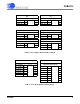
CDB5374 Pin # 1 2 3 4 5 6 7 8 Pin Name P0.1 P0.0 GND D+ DVDD REGIN VBUS Assignment Description SDTKI_MC Token to start CS5376A data transaction SYNC_IO SYNC signal from RS-485 Ground USB differential data transceiver USB differential data transceiver +3.3 V power supply input +5 V power supply input (unused on CDB5374) USB voltage sense input Pin # 9 Assignment RESETz 11 12 13 14 15 16 Pin Name /RST C2CK P3.0 C2D P2.7 P2.6 P2.5 P2.4 P2.3 P2.
CDB5374 Many connections to the C8051F320 microcontroller are inactive by default, but are provided for convenience during custom reprogramming. Listed below are the default active connections to the microcontroller and how they are used. 2.3.4.1 SPI Interface The microcontroller SPI interface communicates with the CS5376A digital filter to write/read configuration information from the SPI 1 port and collect conversion data from the SD port.
CDB5374 input on CDB5374 can receive a lower-frequency system clock and create a synchronous higher-frequency clock using an on-board PLL. Specification Input Clock Frequency Distributed Clock Synchronization Maximum Input Clock Jitter, RMS Value 1.024, 2.048, 4.096 MHz 8.192, 16.384, 32.768 MHz ± 240 ns 1 ns Specification PLL Output Clock Frequency Maximum Output Jitter, RMS Oscillator Type Detector Architecture Value 32.
CDB5374 2.3.6 RS-485 Telemetry By default, CDB5374 communicates with the PC evaluation software through the microcontroller USB port. Additional hardware is designed onto CDB5374 to use the microcontroller I2C® port as a low-level local telemetry, but it is provided for custom programming convenience only and is not directly supported by the CDB5374 PC evaluation software or microcontroller firmware.
CDB5374 A microcontroller software connection is made when the SYNC_MC signal output is created by the microcontroller on command from the system telemetry. The microcontroller can use an internal counter to retime the SYNC_MC signal output to the digital filter SYNC input as required. I2C - SCL, SDA, Bypass 2.3.6.2 The I2C® telemetry connections to CDB5374 transmit and receive through RS-485 twisted pairs.
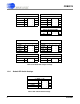
CDB5374 2.3.8 External Connector Power supplies and telemetry signals route to a 20-pin double row connector with 0.1" spacing (J26). This header provides a compact standardized connection to the CDB5374 external signals. Pins 1, 2 3, 4 5, 6 7, 8 9, 10 11, 12 13, 14 15, 16 17, 18 19, 20 2.
CDB5374 Specification Negative Analog Supply, -2.5VA Low Noise Micropower Regulator - Linear Tech Surface Mount Package Type Load Regulation, -40 C to +85 C Quiescent Current, Current @ 100 mA Load Output Voltage Noise, 10 Hz - 100 kHz Ripple Rejection, DC - 200 Hz Value -2.5 V LT1964ES5-BYP SOT-23 +/- 30 mV 30 µA, 1.3 mA 20 µVRMS > 45 dB The VA+ and VA- power supplies to the analog components on CDB5374 can be jumper-ed to use regulated bipolar power supplies (+2.5 V, -2.
CDB5374 The VD and VCORE power supplies on CDB5374 include reverse-biased Schottky diodes to ground to protect against reverse voltages that could latch-up the CMOS components. Also included on VD and VCORE are 100 uF bulk capacitors for bypassing and to help settle transients plus individual 0.1 uF bypass capacitors local to the digital power supply pins of each device. 2.5 2.5.1 PCB Layout Layer Stack CDB5374 layers 1 and 2 are dedicated as analog routing layers.
CDB5374 arated into 4-wire INR+, INF+, INF-, INR- quad groups, and are routed with INF+ and INF- as a traditional differential pair and INR+ and INR- as guard traces outside the respective INF+ and INF- traces. INR+ INR+ INF+ INFINR- INF+ INFINRFigure 5. Quad Group Routing 2.5.3 Bypass Capacitors Each device power supply pin includes 0.1 µF bypass capacitors placed as close as possible to the pin on the back side of the PCB.
CDB5374 2.5.4 Dual Row Headers To simplify signal tracing on CDB5374, all device pins connect to dual-row headers. These dual-row headers are not populated during board manufacture, but the empty PCB footprint exists on the boards and can be used as test points. Figure 7. Dual-row Headers with Shorts The dual-row header pins are shorted on the bottom side of the PCB to pass signals through to the rest of the board.
CDB5374 3. SOFTWARE DESCRIPTION 3.1 Menu Bar The menu bar is always present at the top of the software panels and provides typical File and Help pulldown menus. The menu bar also selects the currently displayed panel. Control Description File Load Data Set Loads a data set from disk. Save Data Set Saves the current data set to disk. Copy Panel to Clipboard Copies a bitmap of the current panel to the clipboard. Print Analysis Screen Prints the full Analysis panel, including statistics fields.
CDB5374 3.2 About Panel The About panel displays copyright information for the Cirrus Seismic Evaluation software. Click OK to exit this panel. Select Help Ö About from the menu bar to display this panel.
CDB5374 3.3 Setup Panel The Setup panel initializes the evaluation system to perform data acquisition. It consists of the following sub-panels and controls.
CDB5374 3.3.1 USB Port The USB Port sub-panel sets up the USB communication interface between the PC and the target board. Control Description Open Target Open USB communication to the target board and read the board name and microcontroller firmware version. When communication is established, the name of this control changes to ‘Close Target’ and Setup, Analysis and Control panel access becomes available in the menu bar. Close Target Disconnects the previously established USB connection.
CDB5374 3.3.2 Digital Filter The Digital Filter sub-panel sets up the digital filter configuration options. By default the Digital Filter sub-panel configures the system to use on-chip coefficients and test bit stream data. The on-chip data can be overwritten by loading custom coefficients and test bit stream data from the Customize sub-panel on the Control panel. Any changes made under this sub-panel will not be applied to the target board until the Configure button is pushed.
CDB5374 3.3.3 Analog Front End The Analog Front End sub-panel configures the amplifier, modulator, and test DAC pin options. Pin options are controlled through the GPIO outputs of the digital filter. Any changes made under this sub-panel will not be applied to the target board until the Configure button is pushed. The Configure button writes the new configuration to the target board and then enables the data Capture button. Control Description Amp Mux Selects the input source for the CS5374 amplifiers.
CDB5374 3.3.5 Gain/Offset The Gain / Offset sub-panel controls the digital filter GAIN and OFFSET registers for each channel. The OFFSET and GAIN registers can be manually written with any 24-bit 2’s complement value from 0x800000 to 0x7FFFFF. The USEGR, USEOR, ORCAL, and EXP[4:0] values enable gain correction, offset correction, and offset calibration in the digital filter. The offset calibration routine built into the digital filter is enabled by writing the ORCAL and EXP[4:0] bits.
CDB5374 3.3.6 Data Capture The Data Capture sub-panel collects samples from the target board and sets analysis parameters. When the Capture button is pressed, the requested number of samples are collected from the target board through the USB port and are split among the enabled channels. A four-channel system, for example, will collect (Total Samples / 4) samples per channel. The maximum number of samples that can be collected is 1,048,576 (1M).
CDB5374 3.3.7 External Macros Macros are generated within the Macros sub-panel on the Control panel. Once a macro has been built it can either be saved with a unique macro name to be run within the Macros sub-panel, or saved as an external macro and be associated with one of the External Macro buttons. A macro is saved as an External Macro by saving it in the . /macros/ subdirectory using the name ‘m1.mac’, ‘m2.mac’, etc.
CDB5374 3.4 Analysis Panel The Analysis panel is used to display the analysis results on collected data. It consists of the following controls.
CDB5374 3.4.1 Test Select The Test Select control sets the type of analysis to be run on the collected data set. Control Description Time Domain Runs a min / max calculation on the collected data set and then plots sample data value vs. sample number. Histogram Runs a histogram calculation on the collected data set and then plots sample occurrence vs. sample value. Only valid for noise data since sine wave data varies over too many codes to plot as a histogram.
CDB5374 3.4.2 Statistics The Statistics control displays calculated statistics for the selected analysis channel. For multichannel data captures, only one channel of calculated statistics are displayed at a time and is selected using the Statistics channel control. Errors that affect statistical calculations will cause the Plot Error control to appear.
CDB5374 3.4.4 Cursor The Cursor control is used to identify a point on the graph using the mouse and then display its plot values. When any point within the plot area of the graph is clicked, the Cursor will snap to the closest plotted point and the plot values for that point display below the graph. When using the Zoom function, the Cursor is used to select the corners of the area to zoom. 3.4.5 Zoom The ZOOM function allows an area on the graph to be expanded.
CDB5374 3.5 Control Panel The Control panel is used to write and read register settings and to send commands to the digital filter. It consists of the following sub-panels and controls.
CDB5374 3.5.1 DF Registers The DF Registers sub-panel writes and reads registers within the digital filter. Digital filter registers control operation of the digital filter and the included hardware peripherals, as described in the digital filter data sheet. Control Description Address Selects a digital filter register. Data Contains the data written to or read from the register. Read Initiates a register read. Write Initiates a register write. 3.5.
CDB5374 3.5.4 Macros The Macros sub-panel is designed to write a large number of registers with a single command. This allows the target evaluation system to be quickly set into a specific state for testing. The Register control gives access to both digital filter registers and SPI1 registers. These registers can be written with data from the Data control, or data can be read and output to a text window.
CDB5374 3.5.6 Customize The Customize sub-panel sends commands to upload custom FIR and IIR filter coefficients, upload custom test bit stream data, start the digital filter, stop the digital filter, and write/read custom EEPROM configuration files to the on-board boot EEPROM. Example data files are included in a sub-directory of the software installation. Control Description Load FIR Coef Write a set of FIR coefficients into the digital filter from a file.
004-00068-Z1 070-00004-Z1 070-00024-Z1 070-00055-Z1 165-00004-Z1 115-00061-Z1 110-00028-Z1 130-00007-Z1 130-00009-Z1 130-00014-Z1 130-00006-Z1 115-00016-Z1 115-00013-Z1 115-00012-Z1 115-00030-Z1 115-00029-Z1 115-00011-Z1 115-00023-Z1 110-00055-Z1 115-00176-Z1 110-00041-Z1 110-00056-Z1 115-00014-Z1 115-00003-Z1 080-00004-Z1 304-00001-Z1 6 7 8 9 10 11 12 13 14 15 16 17 18 19 20 21 22 23 24 25 26 27 28 29 30 31 020-01244-Z1 000-00009-Z1 5 33 001-06603-Z1 4 020-00788-Z1 001-04076-Z1
DS862DB1 Cirrus P/N 020-00934-Z1 020-01130-Z1 020-01074-Z1 020-01128-Z1 020-01104-Z1 000-00001-Z1 020-06288-Z1 021-01391-Z1 020-00673-Z1 020-01048-Z1 020-06253-Z1 000-00002-Z1 020-01016-Z1 120-00002-Z1 120-00011-Z1 060-00195-Z1 060-00063-Z1 061-00062-Z1 060-00062-Z1 065-00178-Z1 060-00162-Z1 060-00236-Z1 065-00287-Z1 065-00173-Z1 065-00056-Z1 060-00067-Z1 061-00064-Z1 062-00022-Z1 062-00055-Z1 062-00079-Z1 061-00061-Z1 060-00175-Z1 080-00003-Z1 300-00025-Z1 102-00017-Z1 070-00005-Z1 240-00355-Z1 603-
CDB5374 5.
CDB5374 DS862DB1 55
CDB5374 56 DS862DB1
CDB5374 DS862DB1 57
CDB5374 58 DS862DB1
CDB5374 DS862DB1 59
CDB5374 60 DS862DB1
CDB5374 DS862DB1 61
CDB5374 6.
CDB5374 DS862DB1 63
CDB5374 64 DS862DB1
CDB5374 DS862DB1 65
CDB5374 66 DS862DB1
CDB5374 DS862DB1 67
CDB5374 68 DS862DB1
CDB5374 DS862DB1 69
CDB5374 70 DS862DB1
CDB5374 DS862DB1 71
CDB5374 72 DS862DB1
CDB5374 DS862DB1 73
CDB5374 74 DS862DB1
CDB5374 DS862DB1 75
CDB5374 76 DS862DB1
CDB5374 DS862DB1 77
CDB5374 78 DS862DB1