
User Manual


6
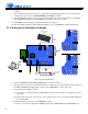
3.1.11.1 Clock and Data Flow for up to 8 Channel ADC inputs
Figure 3-2. Simplified Clock and Data Flow for up to 8 Channel ADC Inputs
The ADC clocking architecture is used when the ADCs are used as the only audio input (i.e. S/PDIF is disabled
as described in Section 4.2.2, “Changing the Audio Input Source” on page 4-3), and the audio input source
multiplexer (U1, U2) is used to select on-board audio sources. Figure 3-2 illustrates this clocking configuration.
The jumpers must be set as described above.
XTAL_OUT from the CS485xx is MCLK for the system. The CS8416 slaves to this MCLK and generates SCLK
and LRCLK for the ADC side of the CS42448 and the DAI side of the DSP.
On the output side, the CS485xx slaves to MCLK from CS8416 and masters SCLK and LRCLK for the DAC side
of the CS42448.
An example of this clocking scheme can be found in pcm_mc_1fs.cpa.
CS42448
2x
CS485XX CS42448
2x
CS8416
MUXED_DSP_SCLK1
DSP_SCLK
DSP_LRCLK
MUXED_DSP_LRCLK1
MUXED_DAI[3:0]
XTAL_OUT
DSP_DA0[3:0]
XMTA S/PDIF OUT
MUXED_MCLK
DAI DAO
SDIN
SDOUT
8
Analog
Inputs
\SPDIF
J100
J101
12CH_ADC
\ON_BRD1\ON_BRD2
HDR1HDR2
Use these jumper settings for the clocking
mode and inputs shown in diagram.