CDB48500 High-performance, 32-Bit Audio Decoder DSP Family CDB48500-USB USB Evaluation Kit Guide Copyright Cirrus Logic, Inc. 2014 (All Rights Reserved) http://www.cirrus.
CDB48500 Contacting Cirrus Logic Support For all product questions and inquiries contact a Cirrus Logic Sales Representative. To find the one nearest to you go to www.cirrus.com IMPORTANT NOTICE “Preliminary” product information describes products that are in production, but for which full characterization data is not yet available. Cirrus Logic, Inc. and its subsidiaries (“Cirrus”) believe that the information contained in this document is accurate and reliable.
CDB48500 Contents Contents . . . . . . . . . . . . . . . . . . . . . . . . . . . . . . . . . . . . . . . . . . . . . . . . . . . . . . . . . . . . . . . . . . . . . . iii Figures . . . . . . . . . . . . . . . . . . . . . . . . . . . . . . . . . . . . . . . . . . . . . . . . . . . . . . . . . . . . . . . . . . . . . . . . . v Chapter 1. Introduction to the CRD48500-USB Evaluation Kit ......................... 1-1 1.1 CDB48500-USB Kit Contents and Requirements . . . . . . . . . . . . . . . . . . . . . . . .
CDB48500 Chapter 4. Configuring the CDB48500 ................................................................ 4-1 4.1 Introduction . . . . . . . . . . . . . . . . . . . . . . . . . . . . . . . . . . . . . . . . . . . . . . . . . . . . . . . . . . . . . . . . 4-1 4.2 Basic Application Download and System Configuration for PCM Pass-through. . . . . . . . 4-1 4.2.1 System Block ................................................................................................................. 4-2 4.2.
CDB48500 Figures Figure 1-1. CDB48500-USB System Block Diagram ......................................................................................... 1-2 Figure 1-2. CDB48500-USB Top View ............................................................................................................... 1-3 Figure 2-1. CDB USB MASTER Driver Setup .................................................................................................... 2-2 Figure 2-2. Board Setup Diagram ...........................
Chapter 1 Introduction to the CRD48500-USB Evaluation Kit 1.1 CDB48500-USB Kit Contents and Requirements 1.1.1 CDB48500-USB Kit Each CDB48500-USB kit comes with the following: • CDB48500 Development Board (See Figure 1-2) • Power Supply: +9V, 1.67A, 100V - 240V, with AC Power Cord • CDB USB MASTER Digital I/O Card (See Figure 1-2) • USB Cable • 3 Board Overlays Identifying the Outputs for CS48520, CS48540, and CS48560 • Document Card Explaining How to Get the Latest Board Software 1.1.
PC USB Port CDB USB MASTER between the PC, CS485XX, and the CDB USB MASTER Serial Control Interface Reset Signals Board Control Signals CDB48500 Audio Data (Future Development) Figure 1-1. CDB48500-USB System Block Diagram This document will concentrate on the features and basic operation of the CDB48500-USB board.
DS784DB2 Copyright 2014 Cirrus Logic Legend: A.CS485XX DSP, U6 B.CS42448 Audio CODEC, U4 C.CS42448 Audio CODEC, U5 D.CS8416 S/PDIF Receiver, U3 E.4 Mbit Serial Flash, U11 F.Headphone jack, J20 G.1/8” Microphone Input Jack, J5 H.Optical S/PDIF Input Jacks (PCM only), J2 I. Coaxial S/PDIF Input Jacks (PCM only), J31 J.Analog Inputs, 2 Vrms Max K.USB Connector on CDB USB Master, L.Alternate +12V Jumper, J3 P1 M.+3.3V Switching Regulator (1.5A), U8 N.+3.
1.2.2 Related Documentation The documents described in this section are updated periodically and may be more up-to-date than the information in this document. Check the Cirrus Logic Internet site for the latest updates. 1.2.2.1 Additional CDB48500 Evaluation Board Information The following information about the CDB48500 Evaluation Board can be obtained from your Cirrus Logic representative: • Schematics • BOM • Artwork and PCB stackup 1.2.2.
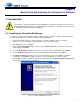
Chapter 2 Board Setup and Installing the Evaluation Kit Software 2.1 Introduction It is important to install the Evaluation Software BEFORE connecting the USB cable from the PC to the CDB USB MASTER card. Failure to install the evaluation software before the initial connection can result in an inability to communicate with the CBD485xx. 2.1.
8. The Opal Kelly Licensing Agreement window will appear next. Click “I Agree” to agree to the terms and continue. 9. The next window asks the user to choose components for installation. By default, only one component is available and is pre-selected – Unified USB Driver. Click Next to continue. 10. The wizard will then ask the user to choose the install location. Select the default location of “C:\Program Files\Opal Kelly\FrontPanel” and click Install. This should take only a few seconds. 11.
B. Connect the other end of the optical cable to the optical output on the back of a DVD player or other digital audio source. 5. Setup Audio Output connections from CDB48500 as follows: A. The RCA connectors labeled AOUT_1A and AOUT_1B are the left and right analog output channels. B. Use the RCA audio cables to connect these line-level analog outputs to powered speakers. 2.1.3 Connecting to a PC Follow these steps to connect to a PC: 1.
Figure 2-5. Found New Hardware Wizard Finish Window 6. It is possible that during the installation, Windows might issue a warning that the drivers have not passed “Windows Logo” testing. Select Continue Anyway. Figure 2-6. Microsoft Windows XP Message Screen 7. Windows should now locate the correct drivers and complete the installation.
2.1.4 Running a Stereo PCM Application on CDB48500-USB To run a stereo PCM application, follow these steps: 1. Launch DSP composer (Start Program Cirrus Logic DSP CS485XXDSP Composer). 2. In DSP Composer, go to File Open and open the appropriate project. 3. Press the GO button 4. Insert PCM material into the DVD player (e.g., music CD). If a DVD is being used as the audio source, make sure that the DVD Player (or other digital audio source) is configured to output PCM data. 5.
Chapter 3 CDB48500 System Description A detailed block diagram of the CDB48500 Customer Development Board is shown in Figure 3-1. The sections that follow provide a detailed description of each block.
3.1 CDB48500 System Block Descriptions 3.1.1 Audio Inputs 3.1.1.1 Analog Line-level Inputs • Connector Type: RCA Female • Absolute Maximum Signal Level: +6.5V • Absolute Minimum Signal Level: GND - 0.7V • Full Scale Amplitude: 2VRMS • Reference Designators: J4, J6-J10, J12, J26-J30, or AIN1A - AIN6B 3.1.1.2 Digital Optical Input Note: Digital Optical Input is PCM only as there is no multi-channel decoder present on CDB48500-USB.
3.1.2.3 Optical Digital Output (PCM) • Connector Type: Fiber Optic TX for Digital Audio, JIS F05 (JIS C5974-1993 F05) • Reference Designator: J24, or SPDIF_TX The S/PDIF output uses the same data line as AOUT_4A and AOUT_4B. When the digital output has been enabled, and you have speakers connected to AOUT_4A and AOUT_4B white noise will be heard. This could damage the speakers. 3.1.
3.1.6 Audio Input Source Multiplexer Selection Headers The CDB48500-USB includes jumpers to change DSP DAI inputs. • Source 0: CDB USB MASTER Board, controlled from Software (Refer to Section 4.2.
3.1.8 CS8416 S/PDIF RX The CS8416 (U3) is a 192 kHz S/PDIF receiver with an integrated input multiplexer. The two S/PDIF input jacks (RXP-RXN) are connected to the CS8416. Only one of the optical or coaxial S/PDIF jacks can be used at a time and is automatically selected by the CS8416. When S/PDIF audio is being processed, the CS8416 must master MCLK for the system (see "Audio Clocking" on page 1-5 for details). 3.1.
3.1.11.1 Clock and Data Flow for up to 8 Channel ADC inputs MUXED_DAI[3:0] MUXED_DSP_LRCLK1 J101 \ON_BRD1 HDR1 MUXED_MCLK \ON_BRD2 HDR2 \SPDIF J100 CS8416 12CH_ADC MUXED_DSP_SCLK1 XTAL_OUT Use these jumper settings for the clocking mode and inputs shown in diagram. SDOUT DAI DAO DSP_SCLK DSP_LRCLK CS485XX DSP_DA0[3:0] SDIN CS42448 CS42448 2x 2x 8 Analog Inputs XMTA S/PDIF OUT Figure 3-2.
3.1.11.2 Clock and Data Flow for S/PDIF Input MUXED_DSP_LRCLK1 J101 MUXED_MCLK \ON_BRD1 HDR1 PLL Use these jumper settings for the clocking mode and inputs shown in diagram. XTAL_OUT DSP_DAI4 HDR2 \SPDIF SPDIF Input J100 S/PDIF Input 12CH_ADC CS8416 \ON_BRD2 MUXED_DSP_SCLK1 SDOUT DAI DAO DSP_SCLK SDIN DSP_LRCLK DSP_DA0[3:0] CS485XX CS42448 CS42448 2x 2x XMTA SPDIF OUT Figure 3-3.
3.1.11.3 Clock and Data Flow for CDB USB Master Card Source MUXED_DAI[4:0] MUXED_DSP_LRCLK1 MUXED_DSP_SCLK1 CDB USB MASTER CARD DAI DAO CS485XX MUXED_MCLK DSP_SCLK DSP_LRCLK SDIN CS42448 CS42448 2x 2x DSP_DA01[3:0] XMTA SPDIF OUT Figure 3-4. CDB USB Master Card Clocking and Data Flow Figure 3-4 illustrates the clocking architecture used when IIS(USB) is used as an audio source, as described in Section 4.2.2, “Changing the Audio Input Source” on page 4-3).
Chapter 4 Configuring the CDB48500 4.1 Introduction The DSP Composer™ software is a graphical user interface (GUI) that is used to program the CS485XX DSP, and to configure the CDB48500. With the exception of the power selection and DAI input jumpers, the CDB48500 is configured exclusively through software. This section provides basic instruction for using the GUI to control the CDB48500, but detailed information can be found in the DSP Composer™ User’s Manual.
4.2.1 System Block The CDB48500 board is populated with a CS48560. However it is possible to evaluate the CS48520, CS48540, CS48560, CS485AU2B, and CS485DV2B on this board. When you drag the system block on to the work space, a popup menu is displayed as shown in Fig. 4-2. This menu lets you choose the target chip that you need to evaluate. When you select the target chip, place the template of the target chip on the analog connectors.
Figure 4-3. Audio In via S/PDIF In 4.2.2.2 Audio In via 8-channel ADC To deliver data to the DSP via 8ch ADC, drag the Audio In block to the work space and select “Analog (8 ch)” as the Input Source. Double click the Audio In block to see the signal flow. The device properties of the Analog (8 ch) element lets you select if the sampling frequency of the ADC on the CS42448 CODEC.
4.2.2.4 DAI Input of CS485xx Each of the Audio In Elements listed above are connected to a DAI element. This represent the DAI port of the DSP. As shown in Fig. 4-5. This dialog allows the user to set the following parameters for the CS485xx: • SCLK Polarity • LRCLK Polarity • Reference Clock - Set to the frequency of the crystal driving the CS485XX(Y1). This is the reference clock is used to determine the clock dividers needed to derive Fs in ADC-only applications.
. Figure 4-6. CDB48500 Digital Audio Output Properties This dialog allows the user to set the following parameters for the CS485XX Audio Output: • LRCLK polarity - Select the phase of LRCLK when the left-sample will be shifted out. • SCLK polarity - Select which edge of SCLK for which the output data will be valid. • DAO1/DAO2 relationship- Select independent or unified clock domains for the DAO1 and DAO2 audio output ports. • MCLK/SCLK Ratios - Select the ratio of LRCLK to MCLK, and LRCLK to SCLK.
. Figure 4-7. Codec DAC Properties This Audio Out dialog allows the user to set the following parameters for the CS42448 DACs: • Audio Data Format -12S or Left-Justified 24-bit • Output Sampling Frequency Range - Select the Fs range where 1FS = 32 kHz, 44.1 kHz, or 48 kHz, 2Fs = 64 kHz, 88.2 kHz, 96 kHz, etc. • Select CODEC/DAC as SCLK and LRCLK Master device. • S/PDIF Enable-Checking this box configures DAO3 for S/PDIF instead of I2S. 4.2.
. Figure 4-8.
4.2.5 Headphone Output The CDB48500 is designed with one Stereo Headphone output. The content of the Headphone output is controlled by the Remap tab in the System Block module. The left right headphone channels match the setttings for DAO-DATA1Left and Right controls on the Remap tab as shown in Fig. 4-9. Figure 4-9. Remap Tab 4.2.6 S/PDIF Transmitter The CDB48500 is designed with one S/PDIF Transmitter output.
Appendix A Schematics A.1 Introduction Updates to the schematics for the CDB48500 Development Board can be can be obtained from your local Cirrus Logic representative as part of a design package including the associated BOM, and layout artwork. The schematics are provided in Adobe’s portable document format (PDF) and PADS™ format. A.1.1 Schematic Pages The schematics included in this document are the original Revision A schematics of the CDB48500 and reflect the board as it was manufactured.
clock domain (MUXED_SCLK, MUXED_LRCLK). On the audio outputs, the CS485XX is slave-only for the MUXED_MCLK master audio clock, and master-only for DSP_SCLK and DSP_LRCLK which are used to shift data out of the CS485XX. The CDB USB MASTER USB board acts as the host controller in the CDB48500 platform, and is connected to the CDB48500 via J11 on page 11 of the schematics. The CDB USB MASTER drives several DSP interfaces including the serial host control port (SCP1), the debug port, and DSP_RESET.
The CS42448_RST signal is a dedicated reset signal driven by a general-purpose output of the CS8416. The CS42448 is a slave to the MUXED_MCLK signal, which is the master audio clock for the entire CDB48500 system. The CS42448 masters the CS8416_SCLK and CS8416_LRCLK signals which are used to shift I2S data out of the CS42448 and shift I2S data into the CS485XX when ADC is used as the data input for the DSP.
A.1.1.1.8 Codec 1 and Codec 2 Input Filters (See Figure 1-8) Each input of the CS42448 has its own input filter that consists of a voltage divider, an AC-coupling capacitor (10 F), and a anti-aliasing capacitor (2700 pF). The voltage divider is provided to make the CDB48500 capable of accepting analog signals of up to 2 VRMS. The CS42448 analog inputs register full-scale for an input amplitude of 1 VRMS. The 12 RCA jacks for analog inputs are also shown on this page. A.1.1.1.
DS784DB2 Copyright 2014 Cirrus Logic A-5 Figure A-1.
DS784DB2 Copyright 2014 Cirrus Logic A-6 Figure A-2.
DS784DB2 Copyright 2014 Cirrus Logic A-7 Figure A-3.
DS784DB2 Copyright 2014 Cirrus Logic Figure A-4.
DS784DB2 Copyright 2014 Cirrus Logic Figure A-5.
DS784DB2 Copyright 2014 Cirrus Logic A-10 Figure A-6.
DS784DB2 Copyright 2014 Cirrus Logic A-11 Figure A-7.
DS784DB2 Copyright 2014 Cirrus Logic A-12 Figure A-8.
DS784DB2 Copyright 2014 Cirrus Logic Figure A-9.
DS784DB2 Copyright 2014 Cirrus Logic A-14 Figure A-10.
DS784DB2 Copyright 2014 Cirrus Logic Figure A-11.
Appendix B Troubleshooting Guide B.1 Intoduction This chapter describes many common problems users may have with the CDB48500-USB, possible causes, and their solutions. B.1.1 Solutions to Possible Problems B.1.1.1 Power LEDs are Not illuminated • DC power supply is not connected to CDB48500 - make sure the DC wall supply is connected to the DC power input jack (J25), and the supply is plugged into a wall outlet.
Revision History Revision DB1 DB2 2 Date Changes September, 2006 Initial release February, 2014 Added Windows 7® to list of PC requirements in Section 1.1.2. Updated project file name in Section 2.1.4. Added CS48560, CS485AU2B, and CS485DV2B to list of chip IDs in Section 4.2.1. Added audio input sources to Section 4.2.2. Updated Fig. 4-8. Updated description of SPP and APP module re-mapping in Section 4.2.6.