
User guide


14 DS723DB1
CDB43L21
4. SYSTEM CONNECTIONS
5. JUMPER SETTINGS
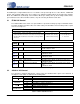
CONNECTOR REF INPUT/OUTPUT SIGNAL PRESENT
+5V J26 Input +5.0 V Power Supply
GND J27 Input Ground Reference
RS232 J95 Input/Output Serial connection to PC for SPI / I²C control port signals
USB J94 Input/Output USB connection to PC for SPI / I²C control port signals
S/PDIF OPTICAL IN OPT1 Input CS8415 digital audio input via optical cable
S/PDIF COAX IN J61 Input CS8415 digital audio input via coaxial cable
I/O Header J5 Input/Output I/O for Clocks & Data
S/W CONTROL J109 Input/Output I/O for external SPI / I²C control port signals
MICRO JTAG J110 Input/Output I/O for programming the micro controller (U84)
FPGA JTAG J78 Input/Output I/O for programming the FPGA (U14)
MICRO RESET S4 Input Reset for the micro controller (U84)
FPGA PROGRAM S2 Input Reload Xilinx Flash program into the FPGA (U14)
H/W BOARD RESET S1 Input Reset for the CS43L21 (U1)
LEFT
RIGHT
J19
J20
Output
RCA phono jacks for analog outputs
SPEAKER +
SPEAKER -
J72
J73
Output Binding Post connected to LM4889 speaker driver for analog out-
puts
Headphone Jack J11 Output Headphone jack for analog outputs
Table 3. System Connections
JMP LABEL PURPOSE POSITION FUNCTION SELECTED
J31 VL
Selects source of voltage for
the VL supply * (Note 1)
*+1.8 V Voltage source is +1.8 V regulator
+2.5 V Voltage source is +2.5 V regulator
+3.3 V Voltage source is +3.3 V regulator
J36 VA_HP
Selects source of voltage for
the VA_HP supply
*+1.8 V Voltage source is +1.8 V regulator
+2.5 V Voltage source is +2.5 V regulator
J25 VA
Selects source of voltage for
the VA supply
*+1.8 V Voltage source is +1.8 V regulator
+2.5 V Voltage source is +2.5 V regulator
J28 VD
Selects source of voltage for
the VD supply
*+1.8 V Voltage source is +1.8 V regulator
+2.5 V Voltage source is +2.5 V regulator
J52
J48
J47
J53
VL
+VA_HP
VA
VD
Current Measurement
*SHUNTED 1 Ω series resistor is shorted
OPEN 1 Ω series resistor in power supply path
J6
Left
Channel
Selects between filtered and
non-filtered output
*AOUTA Connects AOUTA of part directly to LEFT RCA jack
AOUTA (LPF) Connects low-pass filtered AOUTA to LEFT RCA jack
J4
Right
Channel
Selects between filtered and
non-filtered output
*AOUTB Connects AOUTB of part directly to RIGHT RCA jack
AOUTB (LPF) Connects lowpass filtered AOUTA to RIGHT RCA jack
J10
16 ohm
HP LOAD
Load Simulation
SHUNTED 16 Ω resistor shunted from AOUTA to GND
*Not con-
nected
Jumper placed on pin 1
J13
16 ohm
HP LOAD
Load Simulation
SHUNTED 16 Ω resistor shunted from AOUTB to GND
*Not con-
nected
Jumper placed on pin 1
*Default factory settings
Notes: 1. Refer to Section 9 on page 25 regarding jumper settings for J31.
Table 4. Jumper Settings