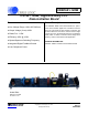
CDB1601-120W CS1601 120W, High-efficiency PFC Demonstration Board Features General Description Line Voltage Range: 108 to 305 VACrms Output Voltage (VLINK): 460V Rated Pout : 115W Efficiency: 95% @ 115W Spread Spectrum Switching Frequency Integrated Digital Feedback Control Low Component Count The CDB1601-120W board demonstrates the performance of the CS1601 digital PFC controller as a standalone unit.
CDB1601-120W IMPORTANT SAFETY INSTRUCTIONS Read and follow all safety instructions prior to using this demonstration board.
CDB1601-120W 1. INTRODUCTION The CS1601 is a high-performance Variable Frequency Discontinuous Conduction Mode (VF-DCM), active Power Factor Correction (PFC) controller, optimized to deliver the lowest PFC system cost for electronic ballast applications. The CS1601 uses a digital control algorithm that is optimized for high efficiency and near unity power factor over a wide input voltage range (108-305 VAC). The CS1601 uses an adaptive digital control algorithm.
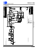
GROUND NEUTRAL 2 3 CHGND RV1 S14K300 NO POP 3.15A SHORT WITH 28 AWG WIRE C1 2200pF SHORT WITH 28 AWG WIRE L5 5mH NO POP 1. ALL RESISTOR VALUES ARE IN OHMS. 2200pF C2 C3 NO POP 0.22uF L1 5mH 2 3 2 NOTES: UNLESS OTHERWISE SPECIFIED; LINE 1 J6 TERM BLK F2 1 4 1 4 45 - 65 Hz 2 3 108-305 VAC 1 2 1 3 2 4 C13 0.22uF L3 1mH 1 4 1 3 2 4 1 - C4 0.47uF NO POP L4 1mH NO POP C5 0.33uF 1.15M R10 1.15M R12 1.
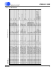
&LUUXV 3 1 070-00157-Z1 011-00042-Z1 011-00055-Z1 011-00040-Z1 013-00034-Z1 012-00186-Z1 001-05280-Z1 001-05783-Z1 001-10233-Z1 001-05542-Z1 001-06276-Z1 011-00064-Z1 070-00132-Z1 070-00166-Z1 070-00001-Z1 180-00022-Z1 311-00019-Z1 115-00014-Z1 110-00301-Z1 110-00302-Z1 080-00013-Z1 050-00039-Z1 050-00050-Z1 040-00127-Z1 040-00127-Z1 050-00039-Z1 050-00047-Z1 304-00004-Z1 071-00107-Z1 020-06337-Z1 020-02502-Z1 020-02616-Z1 020-02273-Z1 020-06390-Z1 020-06310-Z1 030-00091-Z1 030-00091-Z1 020-06356-Z1 020-0
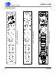
Figure 5. Silkscreen (Top) Figure 4. Solder Mask (Top) Figure 3. Solder Mask (Bottom) CDB1601-120W 4.
DS931DB4 Figure 8. Silkscreen (Bottom) Figure 7. Solder Paste Mask (Bottom) Figure 6.
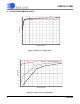
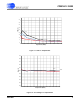
CDB1601-120W 5. TYPICAL PERFORMANCE PLOTS 100 277V 230V 95 120V 90 Efficiency (%) 85 80 75 70 65 60 55 50 10 20 30 40 50 60 70 80 90 100 110 120 Output Power (Watts) Figure 9. Efficiency vs. Output Power 1.00 120V 0.98 230V 0.96 Power Factor 0.94 277V 0.92 0.90 0.88 0.86 0.84 0.82 0.80 20 30 40 50 60 70 80 90 100 110 120 Output Power (Watts) Figure 10. Power Factor vs.
CDB1601-120W 50 45 40 35 THD (%) 30 25 277V 20 15 230V 10 120V 5 0 10 20 30 40 50 60 70 80 90 100 110 120 Output Power (Watts) Figure 11. THD vs. Output Power 470 468 466 464 Vlink (V) 462 277V 230V 460 120V 458 456 454 452 450 0 10 20 30 40 50 60 70 80 90 100 110 120 Output Power (Watts) Figure 12. VLink Voltage vs.
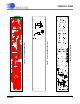
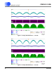
CDB1601-120W Figure 13. Steady State Waveforms — 120 VAC Figure 14.
CDB1601-120W Figure 15.
CDB1601-120W Ch. 1–VLINK Ch. 2–VRECT Ch. 3–Gate Ch. 4–Inductor Current Figure 16. Switching Frequency Profile at Peak of AC Line Voltage — 120 VAC Ch. 1–VDS Ch. 2–VRECT Ch. 3–CS Ch. 4–ZCD Figure 17. Switching Frequency Profile at Peak of AC Line Voltage — 120 VAC (cont.
CDB1601-120W Ch. 1–VLINK Ch. 2–VRECT Ch. 3–Gate Ch. 4–Inductor Current Figure 18. Switching Frequency Profile at Trough of AC Line Voltage —120 VAC Ch. 1–VDS Ch. 2–VRECT Ch. 3–CS Ch. 4–ZCD Figure 19. Switching Frequency Profile at Trough of AC Line Voltage — 120 VAC (cont.
CDB1601-120W Ch. 1–VLINK Ch. 2–VRECT Ch. 3–Gate Ch. 4–Inductor Current Figure 20. Switching Frequency Profile at Peak of AC Line Voltage — 230 VAC Ch. 1–VDS Ch. 2–VRECT Ch. 3–CS Ch. 4–ZCD Figure 21. Switching Frequency Profile at Peak of AC Line Voltage — 230 VAC (cont.
CDB1601-120W Ch. 1–VLINK Ch. 2–VRECT Ch. 3–Gate Ch. 4–Inductor Current Figure 22. Switching Frequency Profile at Trough of AC Line Voltage — 230 VAC Ch. 1–VDS Ch. 2–VRECT Ch. 3–CS Ch. 4–ZCD Figure 23. Switching Frequency Profile at Trough of AC Line Voltage — 230 VAC (cont.
CDB1601-120W Ch. 1–VLINK Ch. 2–VRECT Ch. 3–Gate Ch. 4–Inductor Current Figure 24. Switching Frequency Profile at Peak of AC Line Voltage — 277 VAC Ch. 1–VDS Ch. 2–VRECT Ch. 3–CS Ch. 4–ZCD Figure 25. Switching Frequency Profile at Peak of AC Line Voltage — 277 VAC (cont.
CDB1601-120W Ch. 1–VLINK Ch. 2–VRECT Ch. 3–Gate Ch. 4–Inductor Current Figure 26. Switching Frequency Profile at Trough of AC Line Voltage — 277 VAC Ch. 1–VDS Ch. 2–VRECT Ch. 3–CS Ch. 4–ZCD Figure 27. Switching Frequency Profile at Trough of AC Line Voltage — 277 VAC (cont.
CDB1601-120W Ch. 1–VLINK Ch. 2–VRECT Ch. 3–Gate Ch. 4–Inductor Current Figure 28. Transient — 15W to 115W Load at 10W/s, Vin = 120VAC Ch. 1–VDS Ch. 2–VRECT Ch. 3–CS Ch. 4–ZCD Figure 29. Transient — 15W to 115W Load at 10W/s, Vin = 120VAC (cont.
CDB1601-120W Ch. 1–VLINK Ch. 2–VRECT Ch. 3–Gate Ch. 4–Inductor Current Figure 30. Transient — 15W to 115W Load at 10W/s, Vin = 230VAC Ch. 1–VDS Ch. 2–VRECT Ch. 3–CS Ch. 4–ZCD Figure 31. Transient — 15W to 115W Load at 10W/s, Vin = 230VAC (cont.
CDB1601-120W Ch. 1–VLINK Ch. 2–VRECT Ch. 3–Gate Ch. 4–Inductor Current Figure 32. Transient — 15W to 115W Load at 10W/s, Vin = 277VAC Ch. 1–VDS Ch. 2–VRECT Ch. 3–CS Ch. 4–ZCD Figure 33. Transient — 15W to 115W Load at 10W/s, Vin = 277VAC (cont.
CDB1601-120W Ch. 1–VLINK Ch. 2–VRECT Ch. 3–Gate Ch. 4–Inductor Current Figure 34. Transient — 115W to Zero Load at 10W/s, Vin = 120VAC Ch. 1–VDS Ch. 2–VRECT Ch. 3–CS Ch. 4–ZCD Figure 35. Transient — 115W to Zero Load at 10W/s, Vin = 120VAC (cont.
CDB1601-120W Ch. 1–VLINK Ch. 2–VRECT Ch. 3–Gate Ch. 4–Inductor Current Figure 36. Transient — 115W to Zero Load at 10W/s, Vin = 230VAC Ch. 1–VDS Ch. 2–VRECT Ch. 3–CS Ch. 4–ZCD Figure 37. Transient — 115W to Zero Load at 10W/s, Vin = 230VAC (cont.
CDB1601-120W Ch. 1–VLINK Ch. 2–VRECT Ch. 3–Gate Ch. 4–Inductor Current Figure 38. Transient — 115W to Zero Load at 10W/s, Vin = 277VAC Ch. 1–VDS Ch. 2–VRECT Ch. 3–CS Ch. 4–ZCD Figure 39. Transient — 115W to Zero Load at 10W/s, Vin = 277VAC (cont.
CDB1601-120W 6. REVISION HISTORY Revision 24 Date Changes DB1 FEB 2011 Initial Release. DB2 FEB 2011 Minor BOM change. DB3 MAR 2011 Updated BOM & Layers to rev C. DB4 OCT 2011 Revised part number to reflect lead free.