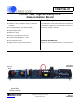
CDB150x-01 CS1501 90W, High-efficiency PFC Demonstration Board Features General Description Variable On Time, Variable Frequency, DCM PFC Controller The CDB150x-01 board demonstrates the performance of the CS1501 digital PFC controller with a 90 watt output at a link voltage of 400 volts. Line Voltage Range: 90 to 265 VAC RMS Output voltage: 400 V Rated Pout: 90 W Efficiency: 97% @ 90 W, 230 VAC No-load Power Dissipation: <0.
CDB150x-01 IMPORTANT SAFETY INSTRUCTIONS Read and follow all safety instructions prior to using this demonstration board. This Engineering Evaluation Unit or Demonstration Board must only be used for assessing IC performance in a laboratory setting. This product is not intended for any other use or incorporation into products for sale. This product must only be used by qualified technicians or professionals who are trained in the safety procedures associated with the use of demonstration boards.
CDB150x-01 1. INTRODUCTION The CS1501 is a high-performance Variable Frequency Discontinuous Conduction Mode (VF-DCM), active Power Factor Correction (PFC) controller, optimized to deliver the lowest system cost in switched mode power supply (SMPS) applications. The CS1501 uses a digital control algorithm that is optimized for high efficiency and near-unity power factor over a wide input voltage range (90-265 VAC).
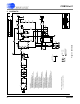
2 4 IND-5MH-TSD-2796 1 3 C2 2200pF C1 2200pF C3 0.22uF Option5 @ U1=NCP1606B:(PIN2=CTRL,PIN3=CT) 1. No populated IC: U2 2. No populated capacitors: C5,C11,C13,C15 3. No populated resistors: R1,R2,R3,R10,R18,R20,R4,R21 4. Shorted components by #28 wire: L4,NTC2 5. Value_changed capacitors: C9=100nF,C8=390nF,C14=1.5nF 6. Value_changed resistors: R13=R14=1M,R15=2M,R17=54.9K,R22=24.9K 7. Value_changed resistors: R6=100K,R9=0.12/1W 8.
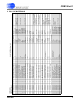
&LUUXV 3 1 070-00157-Z1 011-00042-Z1 011-00055-Z1 011-00064-Z1 011-00040-Z1 013-00034-Z1 012-00191-Z1 000-00009-Z1 001-10233-Z1 001-05280-Z1 001-05542-Z1 001-06035-Z1 001-06035-Z1 110-00301-Z1 110-00302-Z1 070-00132-Z1 070-00154-Z1 070-00001-Z1 180-00025-Z1 311-00019-Z1 080-00013-Z1 050-00039-Z1 050-00039-Z1 040-00127-Z1 040-00127-Z1 050-00051-Z1 304-00004-Z1 036-00008-Z1 036-00008-Z1 071-00083-Z1 020-06374-Z1 000-00004-Z1 020-06376-Z1 020-06389-Z1 020-06310-Z1 030-00092-Z1 021-01186-Z1 020-026
C C C A A 422-00013-01 422-00037-01 603-00473-Z1 240-00473-Z1 600-00473-Z2 080-00036-Z1 080-00002-01 48 49 50 51 52 C C A 300-00025-Z1 47 Rev A A A2 C1 A A Cirrus P/N 020-02502-Z1 110-00025-Z1 065-00328-Z3 065-00276-Z5 036-00006-Z1 311-00025-Z1 Item 41 42 43 44 45 46 CIRRUS LOGIC CDB150X-01_Rev_C WIRE 28/1 AWG, KYNAR MOD, 500FT ASSY DWG CDB150X-0X-Z-NPb PCB CDB150X-0X-Z-NPb SCHEM CDB150X-01-Z-NPb WIRE 22AWG 19/34 STR BLK 105C NP LBL SUBASSY PRODUCT ID AND REV LBL SUBASSY PRODUCT NUMBER
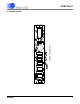
CDB150x-01 Figure 2. Top Silkscreen 4.
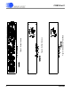
Figure 5. Bottom Solder Paste Mask Figure 4. Bottom Silkscreen Figure 3.
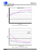
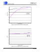
CDB150x-01 5. PERFORMANCE PLOTS Vin=110 Vin=220 99 97 Efficiency(%) 95 93 91 89 87 85 5 6 7 8 9 10 13.5 18 27 36 45 63 90 94.5 Output Power (W) Figure 6. Efficiency vs. Load at 110 VAC, 220 VAC 20 18 16 Vin=110 Vin=220 14 THD(%) 12 10 8 6 4 2 0 10 13.5 18 27 36 45 63 90 94.5 Output Power (W) Figure 7. Distortion vs.
CDB150x-01 1 0.95 Power Factor 0.9 Vin=110 Vin=220 0.85 0.8 0.75 0.7 10 13.5 18 27 36 45 63 90 94.5 Output Power (W) Figure 8. Power Factor vs. Load at 110 VAC, 220 VAC 410 408 406 404 402 VLink (V) Vin=110 Vin=220 400 398 396 394 392 390 1 2 3 4 5 6 7 8 9 10 13.5 18 27 36 45 63 90 94.5 Output Power (W) Figure 9. VLink vs.
CDB150x-01 Figure 10. Steady State Waveforms — 110 VAC Figure 11.
CDB150x-01 Figure 12. Switching Frequency Profile at Trough of AC Line Voltage — 110 VAC Figure 13.
CDB150x-01 Figure 14. Switching Frequency Profile at Peak of AC Line Voltage — 220 VAC Figure 15.
CDB150x-01 Figure 16. Load Transient — 9 W to 90 W, 1 W/uS, 110 VAC Figure 17.
CDB150x-01 Figure 18. Load Transient — 9 W to 90 W, 1 W/uS, 220 VAC Figure 19.
CDB150x-01 6. REVISION HISTORY Revision 16 Date Changes DB1 FEB 2011 Initial Release. DB2 FEB 2011 Updated Efficiency vs. Load plot with more current data. DB3 MAR 2011 Updated BOM & Layers to rev C. DB4 OCT 2011 Revised part number to reflect lead free.