
User guide


8 AN312REV2
AN312
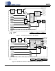
Figure 13. Clock Circuit as Used by Mode 0x04 with CM-1 Module
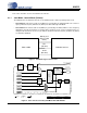
Figure 14. Clock Circuit as Used by Mode 0x04 with CM-2 and Semiconductors
Beat Received
VCXO
24.576MHz
+/- 100 PPM
DAC
MCLK_IN
MCLK_SEL
REFCLK_Enable
REFCLK_Polarity
REFCLK
Edge
Detect
MCLK
MUX
Beat
MUX
Phase
Detector
Sample
Phase
Counter
RST
Loop
Filter
control
Clock
Out
MCLK_OUT (master)
FS1 (word)
SCK (bit)
Audio
Clock
Generator
Clock Config
Signal
Path
Control
Path
Hardware FPGA Software
Active
Signal
Path
Beat Received
VCXO
24.576MHz
+/- 100 PPM
DAC
MCLK_IN
MCLK_SEL
REFCLK
MCLK
MUX
Beat
MUX
Phase
Detector
Sample
Phase
Counter
Loop
Filter
control
Clock
Out
MCLK_OUT (master)
FS1 (word)
SCK (bit)
Audio
Clock
Generator
Clock Config
Signal
Path
Control
Path
External
Hardware
CobraNet
Processor
Software
Active
Signal
Path